Very very good news guys 
http://www.guru3d.com/news-story/intel-core-i7-5960x-de-lidded-haswell-e-uses-soldered-tim.html
http://www.guru3d.com/news-story/intel-core-i7-5960x-de-lidded-haswell-e-uses-soldered-tim.html
Follow along with the video below to see how to install our site as a web app on your home screen.
Note: This feature may not be available in some browsers.
The only one that has been confirmed is 5960x which is the 8-core beast.Does this just apply to the $1,000 version or all of the Haswell-E's, including the 6 core $350 version?
It's interesting to me that the 8 core /16 threads is really a 12 core 24 threaded CPU with 4 cores disabled. Will they disable 1/2 the cores for the 6 core?
glad to see they aren't cutting corners this time with $1k cpus.
Actually, pro's do the 5 point method. One small pea in the center and 4 smaller dots in the corners.This gives a consistent spread with better results,
Alternative is doing a cross. Thin lines from corner to corner. It spreads evenly and does not leave bubbles.
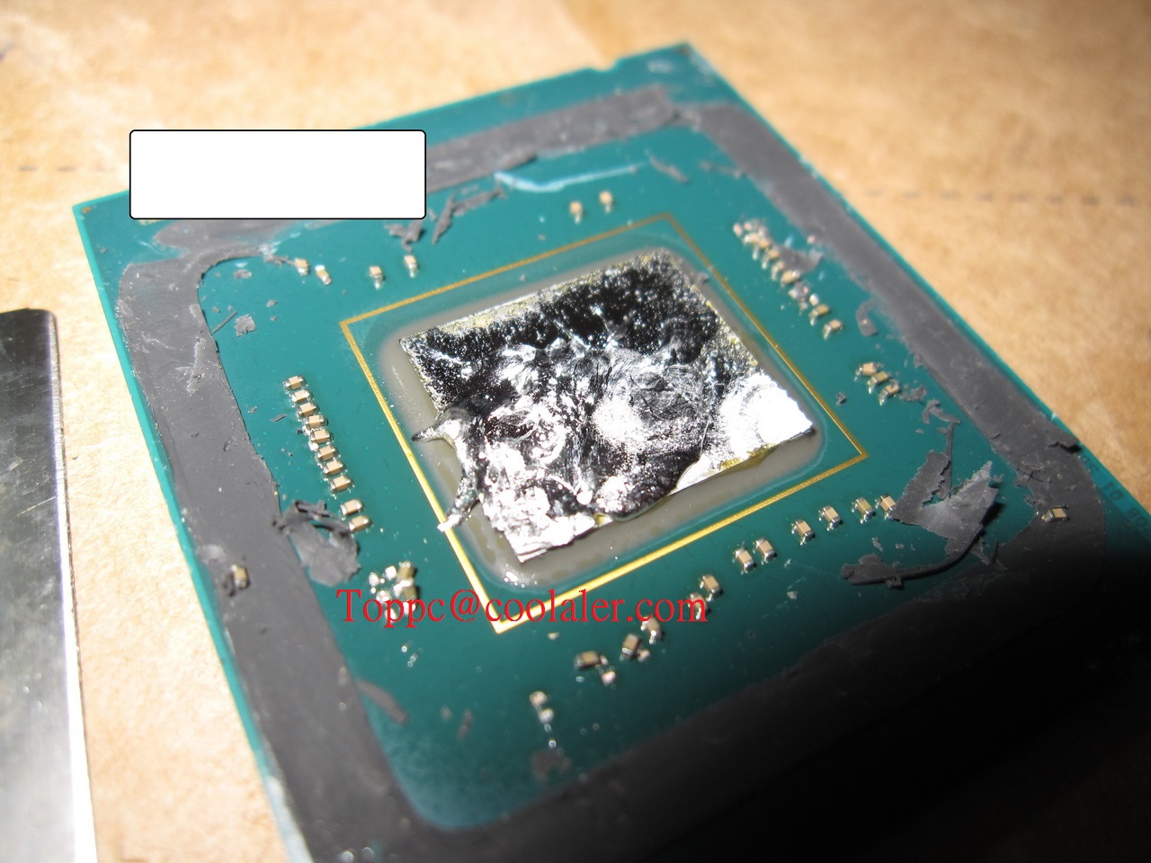
So much for the idea of "you only need a pea of thermal paste in the middle of the heat spreader" when you look at that thing. Cores edge to edge. I knew my method of spreading the paste with a gloved finger was the way to go.
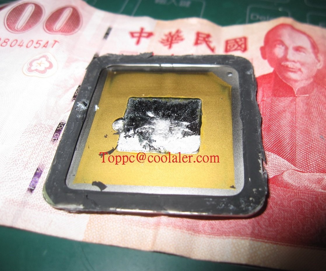
How is a strong epoxy = solder?Haswell-E Uses Soldered Thermal Interface Material
According to what we see in this picture at OCDrift, Intel has started using a strong epoxy between the die of the Core i7-5960X Haswell-E processor and the heat spreader. Thanks to [H] reader Arkanian for the heads up.
How is a strong epoxy = solder?
It's interesting to me that the 8 core /16 threads is really a 12 core 24 threaded CPU with 4 cores disabled. Will they disable 1/2 the cores for the 6 core?
How is a strong epoxy = solder?
now that explaims the rumors of Haswell-E being very poor overclockers: it is a native 12 core design. also soldered die using epoxy could resut in worst thermals than SB-E, IV-E not that any of those were " 5GHz on air" beasts to begin with.
On the other hand this means that we will have a 12-core unlocked chip sooner than expected
epoxy is not "soldering", the same way that Elmers' gluing two pieces of paper together is not "welding"... stupids.
Easy with the stupids.
But this is true. However, it's conflicting. They say "epoxy" but the picture looks like solder in some areas. It's possible it could be some epoxy that when mixed and heated, it turns into a solder (which is the joining of two metals with heat and a filler metal). Kinda like solder paste, but stronger.

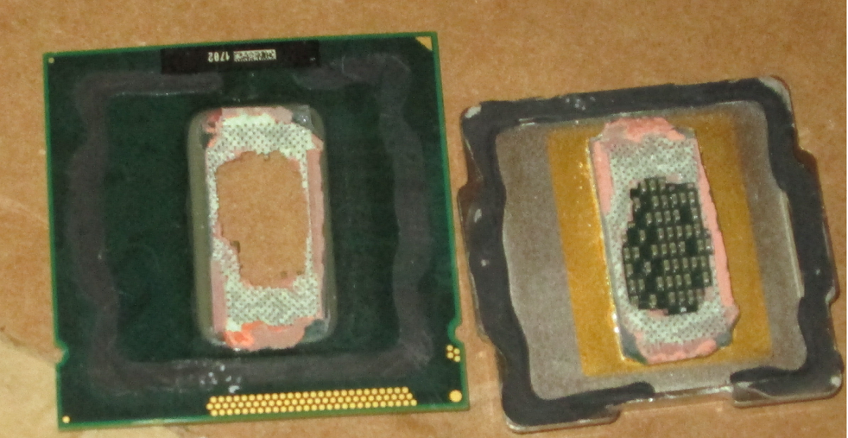
The TIM issues have only been on the 4 core models never a problem on SB-E or IVY-E so I was expecting it to be the same for haswell E and it is.
If it helps, all AMD Phenoms ans FX are soldered.
just watched a newegg video on this and the clock speeds arent very eye catching
3ghz stock and 3.3ghz turbo? ouch on single core performance (95% of apps still single core).
If it helps, all AMD Phenoms ans FX are soldered.
My 4770K got like 61 degrees playing Rift
While my 8350 FX never got that hot and it runs at a higher voltage
Using a simple 212 EVO to cool it