Will Vega be "MidRange" compared to Polaris's "Low Range"?

Zion Halcyon

2[H]4U
Joined
Dec 28, 2007
Messages
2,105
More WCCF rumors, so usual grain of salt caveat, but I think they buried the lead:

AMD’s Waterdrop Strategy Paying Off
These actions had a direct effect on getting the company back in the game. As a newly appointed head of the RTG Raja Koduri quickly began drafting a new strategy and amassing talent. Polaris was the first graphics product born out of a new strategy adopted by the Radeon Technologies Group called Waterdrop.

The idea was to come back to the market with a product whose the sole purpose of was regaining lost market share as quickly as possible. To do that Raja had to come up with a product that the vast majority of PC gamers would want to buy and, most importantly, can afford. This meant breaking away from the historical trend that both AMD & Nvidia followed of launching the fastest and most powerful product in the lineup first and following up with more mid-range and mainstream options later.

...

The Radeon Technologies Group’s plan is to introduce HBM2 technology with the upcoming VEGA graphics architecture across more market segments compared to where the first generation of the technology currently exists. Which is confined only to the highest end segment of the market. If everything goes according to plan VEGA will be the first architecture to bring High Bandwidth Memory technology to more affordable products further down the stack.

Read more: AMD Takes Graphics Share From Nvidia For The Fourth Consecutive Quarter


​

Frankly, in the given context, it almost reads like Vega is due to underperform as well, so they are going to aim to bring HBM2 to midrange cards.

We may indeed not see a top end competitor for AMD until Navi.
 
I think they should stop at the $499 price point. Let Nvidia have the luxury suite to themselves. Maybe dabble with some IoT uses for their SoC designs. Would be cool if they could interface with a Master PC in the home like the Thunderbolt case for GPU. Stuff like that.
 
I think they should stop at the $499 price point. Let Nvidia have the luxury suite to themselves. Maybe dabble with some IoT uses for their SoC designs. Would be cool if they could interface with a Master PC in the home like the Thunderbolt case for GPU. Stuff like that.

They might just.

I know Raja is particularly big on getting mGPU working - if they can do that, perhaps they figure they can compete then by "just adding more gpus".

Not sure how that would work exactly, given SLI and Crossfire have their warts, but Explicit is supposed to have an advantage over those implicit options.
 
You are assuming too much. Vega is not just one part. Vega will be the lineup and of course there will be a kid range part. They are not just going to release one Vega part. There are multiple Vega chips. Vega 10 and. Vega 11.
More WCCF rumors, so usual grain of salt caveat, but I think they buried the lead:

AMD’s Waterdrop Strategy Paying Off
These actions had a direct effect on getting the company back in the game. As a newly appointed head of the RTG Raja Koduri quickly began drafting a new strategy and amassing talent. Polaris was the first graphics product born out of a new strategy adopted by the Radeon Technologies Group called Waterdrop.

The idea was to come back to the market with a product whose the sole purpose of was regaining lost market share as quickly as possible. To do that Raja had to come up with a product that the vast majority of PC gamers would want to buy and, most importantly, can afford. This meant breaking away from the historical trend that both AMD & Nvidia followed of launching the fastest and most powerful product in the lineup first and following up with more mid-range and mainstream options later.

...

The Radeon Technologies Group’s plan is to introduce HBM2 technology with the upcoming VEGA graphics architecture across more market segments compared to where the first generation of the technology currently exists. Which is confined only to the highest end segment of the market. If everything goes according to plan VEGA will be the first architecture to bring High Bandwidth Memory technology to more affordable products further down the stack.

Read more: AMD Takes Graphics Share From Nvidia For The Fourth Consecutive Quarter


​

Frankly, in the given context, it almost reads like Vega is due to underperform as well, so they are going to aim to bring HBM2 to midrange cards.

We may indeed not see a top end competitor for AMD until Navi.
ega
 
You are assuming too much. Vega is not just one part. Vega will be the lineup and of course there will be a kid range part. They are not just going to release one Vega part. There are multiple Vega chips. Vega 10 and. Vega 11.

ega

This is exactly what I was thinking but could not think how to put it into words. I just figured that if Vega was according to plan, that would then be the start of where they could start using HBM2 in lower tiered products.
 
The real question is just how large of a board/interposer you can make if chaining together chips with a fast interconnect. The same concept of wide IO that makes HBM feasible with the interposer would also apply to the processors. Crossfire and SLI were invented because care had to be taken to work around the limited bandwidth of any interconnect. I'd still predict a midrange and high/enthusiast class Vega. The mid would also need sized appropriately for APUs. I wouldn't expect a low end part until that cheap HBM that was discussed the other day is available. HPC Zens with mid/high GPUs attached would offer significant benefits to the server and HPC communities for a lot of worksets. Just having the HBM and not even using the GPU would be a huge advantage for some workloads. I'm also not expecting scaling much past what we see with current Crossfire setups. So two-way, maybe four-way, configurations to make higher tier products. Navi I'd expect to change that where maybe it's a matter of affixing SMs, ACEs, etc as discrete chips.
 
The real question is just how large of a board/interposer you can make if chaining together chips with a fast interconnect. The same concept of wide IO that makes HBM feasible with the interposer would also apply to the processors. Crossfire and SLI were invented because care had to be taken to work around the limited bandwidth of any interconnect. I'd still predict a midrange and high/enthusiast class Vega. The mid would also need sized appropriately for APUs. I wouldn't expect a low end part until that cheap HBM that was discussed the other day is available. HPC Zens with mid/high GPUs attached would offer significant benefits to the server and HPC communities for a lot of worksets. Just having the HBM and not even using the GPU would be a huge advantage for some workloads. I'm also not expecting scaling much past what we see with current Crossfire setups. So two-way, maybe four-way, configurations to make higher tier products. Navi I'd expect to change that where maybe it's a matter of affixing SMs, ACEs, etc as discrete chips.

I don't think you'd even be able to fit four stacks of HBM and two P10 dies on an interposer. What configuration would you need for such a scheme to be less expensive than a single larger die?

Fiji was already pushing reticle size limit, and two 300mm dies will take up more space than one 600mm
 
More WCCF rumors, so usual grain of salt caveat, but I think they buried the lead:

AMD’s Waterdrop Strategy Paying Off
These actions had a direct effect on getting the company back in the game. As a newly appointed head of the RTG Raja Koduri quickly began drafting a new strategy and amassing talent. Polaris was the first graphics product born out of a new strategy adopted by the Radeon Technologies Group called Waterdrop.

The idea was to come back to the market with a product whose the sole purpose of was regaining lost market share as quickly as possible. To do that Raja had to come up with a product that the vast majority of PC gamers would want to buy and, most importantly, can afford. This meant breaking away from the historical trend that both AMD & Nvidia followed of launching the fastest and most powerful product in the lineup first and following up with more mid-range and mainstream options later.

...

The Radeon Technologies Group’s plan is to introduce HBM2 technology with the upcoming VEGA graphics architecture across more market segments compared to where the first generation of the technology currently exists. Which is confined only to the highest end segment of the market. If everything goes according to plan VEGA will be the first architecture to bring High Bandwidth Memory technology to more affordable products further down the stack.

Read more: AMD Takes Graphics Share From Nvidia For The Fourth Consecutive Quarter


​

Frankly, in the given context, it almost reads like Vega is due to underperform as well, so they are going to aim to bring HBM2 to midrange cards.

We may indeed not see a top end competitor for AMD until Navi.
Navi is just bringing their CPU strategy to the GPU market, trying to solve performance deficits by throwing more cores at it. With the realities of DX12 and how much AMD likes to be hands-off in game development I don't think we'll ever see good scaling to make Navi a real competitor, especially in the high-end and enthusiast markets.
 
Navi is just bringing their CPU strategy to the GPU market, trying to solve performance deficits by throwing more cores at it. With the realities of DX12 and how much AMD likes to be hands-off in game development I don't think we'll ever see good scaling to make Navi a real competitor, especially in the high-end and enthusiast markets.

I don't understand are you talking about multiple dies on an interconnect or about the number of CUs going up?
 
multiple dies/chips on an interconnect that is what Navi is supposed to be, the reality is, GPU's won't get the same "benefits" as CPU since they are already very parallel.

The big difference is R&D to create the bigger chip, the cost and yield of new processes.

Once a chip is taped out, manufacturing the chip on a new node is expensive, the bigger the die, the less yields you have of fully functional chips. Mainly because of growth errors and process errors. Now as the process matures process errors drop so bigger chips become more viable. The small die strategy works great at the beginning of a new process and a new chip design but the costs have to be weighed out with the cost of the transposer and cost of assemble vs the loss due to silicon errors (added to this you have to factor in the different sku's of cut down parts as well on both strategies) and the progression of mGPU performance of all software, over the entire life time of production.

In the short term its a good strategy (saves money via R&D expense, cost of manufacturing expense) but in the long term, its a strategy of diminishing returns unless mGPU is well adopted by majority of the developers which frankly we would have seen with Xfire and Sli, but rendering technology and what is available for horsepower dictated that wasn't going to happen.

What I think the strategy really is for, is to cut down immediate costs, while still gaining marketshare so they can return to large chips again, like they did in the past. Yes we have seen this strategy before by AMD, after the r600 debacle, with the spin of mGPU.
 
Last edited:
I don't understand why anyone cares about HBM as a selling point. If it improves performance above what GDDR5X can provide then great, I'm all for it. But designing a part to use HBM just to add an extra feature on the box seems like a dumb idea. I'd be curious to see if producing HBM parts is actually cheaper when you consider the costs of the memory itself and the interposer. The PCB can be smaller and more compact, sure, but I don't know if that's still a net savings or not.
 
multiple dies/chips on a interconnect that is what Navi is supposed to be, the reality is, GPU's won't get the same "benefits" as CPU since they are already very parallel.

The big difference is R&D to create the bigger chip, the cost and yield of new processes.

Once a chip is taped out, manufacturing the chip on a new node is expensive, the bigger the die, the less yields you have of fully functional chips. Mainly because of growth errors and process errors. Now as the process matures process errors drop so bigger chips become more viable. The small die strategy works great at the beginning of a new process and a new chip design but the costs have to be weighed out with the cost of the transposer and cost of assemble vs the loss due to silicon errors (added to this you have to factor in the different sku's of cut down parts as well one both strategies) and the progression of mGPU performance of all software, over the entire life time of production.

In the short term its a good strategy (saves money via R&D expense, cost of manufacturing expense) but in the long term, its a strategy of diminishing returns unless mGPU is well adopted by majority of the developers which frankly we would have seen with Xfire and Sli, but rendering technology and what is available for horsepower dictated that wasn't going to happen.

What I think the strategy really is for, is to cut down immediate costs, while still gaining marketshare so they can return to large chips again, like they did in the past. Yes we have seen this strategy before by AMD, after the r600 debacle, with the spin of mGPU.

I would assume if they do it on an interpose they could make it transparent to the API otherwise it's a total crapshoot on a very expensive product. Yields could be a factor yes, but you'd would introduce more waste in the form of the interposer; if any of the dies (hbm and gpus) have any issues whatsoever that's all going to waste :p Plus how big are these interposers going to get exactly, I just don't see this happening. A better interconnect for mGPU I can understand though, and that may well be possible next year.
 
I would assume if they do it on an interpose they could make it transparent to the API otherwise it's a total crapshoot on a very expensive product. Yields could be a factor yes, but you'd would introduce more waste in the form of the interposer; if any of the dies (hbm and gpus) have any issues whatsoever that's all going to waste :p Plus how big are these interposers going to get exactly, I just don't see this happening. A better interconnect for mGPU I can understand though, and that may well be possible next year.


It can't be transparent to the API, its a function of what each individual unit is doing, the only way to get around that is if the command processors of one GPU knows what the other command processors of the other GPU is doing, which kinda of defeats the purpose of having multiple GPU's lol, If they break out the command processors from the other parts of the gpu into its own chip that might work, but that will introduce high latency, and cache I don't think can cover that as you will be forced to use l2 global. This will be like having a CPU controlling what the GPU's do, so ya end up with the same thing you are trying to avoid lol.
 
It can't be transparent to the API, its a function of what each individual unit is doing, the only way to get around that is if the command processors of one GPU knows what the other command processors of the other GPU is doing, which kinda of defeats the purpose of having multiple GPU's lol, If they break out the command processors from the other parts of the gpu into its own chip that might work, but that will introduce high latency, and cache I don't think can cover that as you will be forced to use l2 global. This will be like having a CPU controlling what the GPU's do, so ya end up with the same thing you are trying to avoid lol.

Yeah that's having some sort of unified command processor is what I was thinking of, it makes no sense at all to commit to sticking two GPUs and memory on an interposer if you're not 100% it's going to scale all the time so I think multi-GPU on interposers is a dead end.
 
Fiji was already pushing reticle size limit, and two 300mm dies will take up more space than one 600mm
True, but yields will be significantly higher and you could push past that 600mm limit.

I don't think you'd even be able to fit four stacks of HBM and two P10 dies on an interposer. What configuration would you need for such a scheme to be less expensive than a single larger die?
Not sure you would need 4 stacks. 2 or 3 might be sufficient unless you really need a large memory pool. Consider P100 with 4 stacks and the cost of an interposer isn't really a concern at that level.

In the short term its a good strategy (saves money via R&D expense, cost of manufacturing expense) but in the long term, its a strategy of diminishing returns unless mGPU is well adopted by majority of the developers which frankly we would have seen with Xfire and Sli, but rendering technology and what is available for horsepower dictated that wasn't going to happen.
The key here is that traditional mGPU won't be required with the interconnect. It only exists because "Large Resource A" needs to be accessed on GPU B. With a 100GB/s link and ability to address memory on the other side that's less of an issue. They may each still be working on independent frames, and fences could be tricky, but most of the synchronization should no longer be an issue as resources don't need moved back and forth.

I don't understand why anyone cares about HBM as a selling point. If it improves performance above what GDDR5X can provide then great, I'm all for it. But designing a part to use HBM just to add an extra feature on the box seems like a dumb idea. I'd be curious to see if producing HBM parts is actually cheaper when you consider the costs of the memory itself and the interposer. The PCB can be smaller and more compact, sure, but I don't know if that's still a net savings or not.
The only nice thing about HBM over GDDR5 is the form factor of the board. You simply end up with a smaller card which matters to some people. The performance side should be better than GDDR5/X as well, but we haven't really seen a configuration with only as much bandwidth as GDDR5 provides. Fury still exists in it's own ballpark even with all the Pascal cards, excluding P100 which isn't really a GPU. HBM will never be cheaper than GDDR5, but it provides options unavailable to GDDR5.

I would assume if they do it on an interpose they could make it transparent to the API otherwise it's a total crapshoot on a very expensive product. Yields could be a factor yes, but you'd would introduce more waste in the form of the interposer; if any of the dies (hbm and gpus) have any issues whatsoever that's all going to waste :p Plus how big are these interposers going to get exactly, I just don't see this happening. A better interconnect for mGPU I can understand though, and that may well be possible next year.
Yeah the goal would be transparent mGPU. Where it was entirely abstracted away from the API. With how the frontend on GCN currently works it should be possible as most scheduling is in hardware and cache used for synchronization. As for wasted parts, bad parts will be discarded or binned independently of the full setup. Issues should only arise from misaligned parts. As was mentioned with the low cost HBM, simply spacing the TSVs differently and allowing bigger pads can address some of those concerns. It's probably possible to remove bad parts once assembled, but no idea what kind of costs that would entail.

It can't be transparent to the API, its a function of what each individual unit is doing, the only way to get around that is if the command processors of one GPU knows what the other command processors of the other GPU is doing, which kinda of defeats the purpose of having multiple GPU's lol, If they break out the command processors from the other parts of the gpu into its own chip that might work, but that will introduce high latency, and cache I don't think can cover that as you will be forced to use l2 global. This will be like having a CPU controlling what the GPU's do, so ya end up with the same thing you are trying to avoid lol.
With a low level API it could be largely transparent. It should only be an issue if the app somehow waited for the current scene to finish rendering before firing off or queuing the next. At which point all cards are likely to have poor performance regardless. It only has to stop if a resource is needed from the other card, but that issue is largely addressed with the interconnect.

There could be several ways to handle the command processor. One could be disabled or slaved to the other. Or they each work independently with fences synchronizing when a resource is disabled. Not too unlike how it's handled now where you can't continue until one stage completes. Think concurrent execution with graphics+graphics instead of just graphics+compute. No technical reason you would have only a single graphics or compute queue. Just have multiple graphics queues with synchronization between them.
 
The key here is that traditional mGPU won't be required with the interconnect. It only exists because "Large Resource A" needs to be accessed on GPU B. With a 100GB/s link and ability to address memory on the other side that's less of an issue. They may each still be working on independent frames, and fences could be tricky, but most of the synchronization should no longer be an issue as resources don't need moved back and forth.

With a low level API it could be largely transparent. It should only be an issue if the app somehow waited for the current scene to finish rendering before firing off or queuing the next. At which point all cards are likely to have poor performance regardless. It only has to stop if a resource is needed from the other card, but that issue is largely addressed with the interconnect.

There could be several ways to handle the command processor. One could be disabled or slaved to the other. Or they each work independently with fences synchronizing when a resource is disabled. Not too unlike how it's handled now where you can't continue until one stage completes. Think concurrent execution with graphics+graphics instead of just graphics+compute. No technical reason you would have only a single graphics or compute queue. Just have multiple graphics queues with synchronization between them.


That isn't being transparent to the API, using fences which are part of the API and telling the command processors what is coming first and then what is coming next.

Slaving the command processors to one or the other, you will have issues as you need to disseminate all information from one processor to another, so you will need one chip that is "more capable" from a scheduling point. Which at that point you will have no need of the other command processors. And this goes back to the original problem, bandwidth needs. Yes being on an interposer you have greater bandwidth to access from, but by doing so, you still have the problem with using slower cache.
 
If the top Vega chip is below a 1080, it will be a failure in my AMD fanboys eyes. It needs to beat that card at a MINIMUM. It's ok if it fails to beat a titan or 1080ti as at least those cards were meant to be fully fleshed out higher end cards taking up more die space, but if a 400mm amd vega chip can't even beat a 3xx mm pascal chip, that's a disaster.

AMD should undercut nvidia no matter what the performance turns out to be though, they need to go for nvidias throats, more marketshare, if that means less asp, so be it.
 
if its using HBM 2 its going to be hard to undercut...... I would rather see them in a position to grow margins, than have them have the top or equal spot with crazy power consumption; with in 15% would be great for both power and performance. 31% margins is not good, they should be at least 35%, ideally at 40%. Granted most of that is due to their CPU side but we know Polaris is around that level too.
 
Last edited:
That isn't being transparent to the API, using fences which are part of the API and telling the command processors what is coming first and then what is coming next.
Fences still have to be interpreted by the driver. The issues are easily resolved the same way compute queues are now. The only difference is where the signaling goes. GCN already has hardware schedulers that handle dependencies, in some cases for real time scheduling.

Slaving the command processors to one or the other, you will have issues as you need to disseminate all information from one processor to another, so you will need one chip that is "more capable" from a scheduling point. Which at that point you will have no need of the other command processors. And this goes back to the original problem, bandwidth needs. Yes being on an interposer you have greater bandwidth to access from, but by doing so, you still have the problem with using slower cache.
The synchronization seems like it would be very similar to how compute and graphics are handled currently. It's just a matter of if it's handled in hardware or by the driver.
 
Fences still have to be interpreted by the driver. The issues are easily resolved the same way compute queues are now. The only difference is where the signaling goes. GCN already has hardware schedulers that handle dependencies, in some cases for real time scheduling.

Fences and barriers are constructs of the API, yeah the driver has to be involved to interpret them that is natural.


The synchronization seems like it would be very similar to how compute and graphics are handled currently. It's just a matter of if it's handled in hardware or by the driver.

You will be going out of the way to do this in the driver, the driver is essential the CPU, you don't want to do it that way, its the same issue with SLi and Xfire and hence why they have more CPU overhead. If you want the ability to have mGPU seemless and invisible to the programmer, you can't use the current mGPU methods nor do you want the driver/CPU involved to this extent. Raja are stated the issues with mGPU and how developers have to change their mindset when it comes to programing for it. Its something developers have to do which coincidentally is very similar to SLi and Xfire needs, but technology (horsepower and renderers) have not been able to do this effectively yet. MS decided to remove Sli and Xfire as marketing for either camp.
 
Fences and barriers are constructs of the API, yeah the driver has to be involved to interpret them that is natural.
Driver doesn't have to be involved. In the case of GCN the ACEs or HWS can track the signals and the driver wouldn't need to do anything. Simply keep polling a register to see if it's time to continue. Even that would ultimately be unnecessary if there were pins connecting the schedulers on all chips. I think I saw a paper somewhere that XB1 had 2 GCPs. So they could probably partition the chip into halves and use that for effectively testing multiple chips. There are so many ways they could theoretically approach this there is no real reason to even speculate on it. As for Raja and developers, that may have more to do with SFR and dealing with heterogeneous adapters. Use the APUs alongside the GPU primarily for compositing.
 
ah no, something has to be controlling the ACE's and HWS's that's how it works with GCN, look at the white papers for GCN, the ACE's and HWS's are only part of the control silicon, they don't not work independently.

And Raja stated it was work to be done before Navi, so Navi could be successful.
 
Vega will be Vega 10 and Vega 11 which one could be HBM2 with HBM specs or HBM2, or just GDDR5 with bigger bus width.

and Navi clearly shows it will have Scalability and Next Gen memory, Either can be Scalability on architecture changes like using more SEs,RBEs,Rasterizers,Geometry Engines,Etc. and also increasing stack height on HBM.even changing some details in GCN

I don't understand why anyone cares about HBM as a selling point. If it improves performance above what GDDR5X can provide then great, I'm all for it. But designing a part to use HBM just to add an extra feature on the box seems like a dumb idea. I'd be curious to see if producing HBM parts is actually cheaper when you consider the costs of the memory itself and the interposer. The PCB can be smaller and more compact, sure, but I don't know if that's still a net savings or not.
HBM compared to GDDR5X which was released some months ealier Redudes power consumption,latency,increases the Bandwidth and density per area
 
Last edited:
HBM compared to GDDR5X which was released some months ealier Redudes power consumption,latency,increases the Bandwidth and density per area
I know this. It has performance benefits when you are bandwidth constrained, and it can produce smaller boards. However I was responding to this comment:
The Radeon Technologies Group’s plan is to introduce HBM2 technology with the upcoming VEGA graphics architecture across more market segments compared to where the first generation of the technology currently exists.
Simply aiming to bring it to more markets for it's own sake doesn't make sense. There would have to be either a cost advantage or a performance advantage.
 
ah no, something has to be controlling the ACE's and HWS's that's how it works with GCN, look at the white papers for GCN, the ACE's and HWS's are only part of the control silicon, they don't not work independently.

And Raja stated it was work to be done before Navi, so Navi could be successful.
Except they don't need the CPU to perform their scheduling. Look at the slides AMD released regarding realtime scheduling. Yes the CPU has to create the initial load, but they can manage some of the synchronization on their own. So if one frame signals that it is finished the HWS(I'm assuming over ACE here) can can start the next frame that was queued with no CPU interaction. I'm sure a signal goes to the CPU as well, but it wouldn't be required to proceed. For audio they tied it to an internal clock so they could fill audio buffers without having to interrupt the CPU. So ultimately it depends if the app was submitting tasks in a blocking or non-blocking style.
 
look you are simplifying it too much, if it was that easy it would have already been done with polaris and they would have came out with a performance part, with 2 polaris's on one interposer clocked lower and it would have matched a 1070 or might even go up to the 1080 at a reasonably higher power consumption, if they could do that.

No it isn't that simple, and it never will be. I don't understand why you think something like this is like a turning on a switch, its not like AMD wants to loose hundreds of millions of dollars or to give nV hundreds of millions of dollars.....

And I didn't say they "need another CPU" I said its "like" having another CPU which defeats the purpose of having two dies on substrate in the first place so it won't be done that way.
 
Always has to be at least one.

I'm no AMD basher. I run an AMD system (8350/390) but I also call a spade a spade. Polaris is positioned in the only place it could be. Polaris fell short and because it did there is nothing for a gamer in this generation of GPUs that likes the $350 or so price point like I do. Maybe Vega fixes that.
 
In the short term its a good strategy (saves money via R&D expense, cost of manufacturing expense) but in the long term, its a strategy of diminishing returns unless mGPU is well adopted by majority of the developers which frankly we would have seen with Xfire and Sli, but rendering technology and what is available for horsepower dictated that wasn't going to happen.

Yes and no. They really aren't the same thing. There is a lot to be gained because of things like unified heterogenious memory architecture. Remember with SLI/X-Fire you had to apply patches to force things like buffer updates. This often happened when the two frame buffers got out of sync and caused problems. And this syncing is the fact you were still dealing with the same amount of memory (didn't composite) created the scaling issues. (That and your PCIe bus was now divided which made loading of high res textures and models twice as expensive) So SLI/X-Fire was sort of like working in Parallel with large amounts of data duplciation. The mGPU concept is more like working in serial with more available resources on tap at once.

Nuvi may make GPU resources look like one giant GPU to the drivers. If Nuvi can interconnect all the GPU's with the memory there are some large scaling gains to be seen here. Like I said in previous post, it's all about how the scheduler chip hands out instructions and handles memory.
 
Navi's interconnect will be similar to Omni path by Intel, and nV's nVlink, it won't be able to make it look like there is only one chip. This is why Raja stated it is very important to get developers to change the way they program. Now Intel can do it differently because their co processor is a CPU, but its not very good with graphics so......

The problem doesn't show on the memory side, the problem is with what GPU units are doing what. And this is why neither company has tried do multiple GPU and glue them together in any form because that problem will still exist.

The new bus will take away the bandwidth stops and the intercommunication latency between the two GPU's, but it won't stop the initial problem which is much harder to solve, as you can't slave one chip to another as I mentioned before (in essence, SLI and Xfire you do have a master and slave device but are controlled by the driver via the CPU). There still needs to be explicit programming involved to ensure things go smoothly.
 
I'm no AMD basher. I run an AMD system (8350/390) but I also call a spade a spade. Polaris is positioned in the only place it could be. Polaris fell short and because it did there is nothing for a gamer in this generation of GPUs that likes the $350 or so price point like I do. Maybe Vega fixes that.

It appears to me, despite your choice in hardware, that you are taking the information out of context. I doubt very much that Polaris fell short although I am sure if they could have had it go faster, they would have preferred that. However, RTG already knew from the beginning what they were aiming for with this release and they appear to have done so. (Especially with the RX 470.)

The fact that RTG is in many ways a new company with a new direction, what they are doing makes sense in its proper context. Vega is for the near future but, what good is Vega if AMD does not get more market share now well they can. Also, the fact that their discrete market share has gone up to just over 29% without the Polaris architecture seems that the strategy is working, at least in the short term. (I beat they have sold a lot of R9 390's. :) )

They are options from AMD for the over $350 crowd but, it is from the last generation and they are now more cost effective than ever before. (I have an R9 Fury Nitro+.) Market share is more important than large profits for AMD in the short term but, in the long term, larger profits are definitely needed for R&D.
 
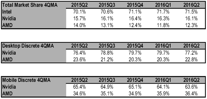
They did NOT sell discrete desktop units much more than before, the marketshare gain was due to notebook discrete gains.

Please look at the numbers break down. AMD gained more points on notebooks, which combined with the 4.8% gain over 4 quarters of the desktop constituted a 12% gain when looking at the entire market of notebook and desktop GPU's,

Notebook share swings are normal, we have seen 20 point swings to either IHV over one quarter, desktop marketshare rarely swings, even 10% is a huge swing in desktop numbers per quarter, this is because brand loyalty is much less on the notebook side and what ever is cheaper for the OEM and end user is what matters more.

This is why gaining 5% per quarter for AMD, would be great, on the desktop side of things, but realistically 2.5% is more likely.

As much as it "looks" like RTG is a different company apart from AMD or their division looks different, they still have to answer to AMD's board, and the pool of resources is still dictated by the board, so there seems to be some change, but that change could just be fascia for all we know.

Marketshare and profits are both important. It matters if ya have 50% marketshare but ya got 10% margins, and your competitor has the other half of the marketshare and they have 50% margins. You can see what happens when margins drop, look at the the time 2xx line from nV came out, they were forced to cut margins because of the 4xxx line from AMD and that hurt nV's bottom line greatly, I think they had the first loss since the FX series. But they still were no where near the marketshare disparity AMD is at now.

Everyone knows AMD needs marketshare but they can't do it at the expensive of margins and ASP's.

Having said that, older products yeah get rid of them at low margins cause its better to do that than taking a write off.

This is why I call WCCF tech, WTF tech,

9047df6d-e8c5-4b43-8296-714959ec3563.png


These are the correct numbers, WTF tech just didn't read the numbers right or making shit up or they are mixing numbers for JPR and Mercury which I don't see how, they just seem fabricated.
 
Last edited:
I know this. It has performance benefits when you are bandwidth constrained, and it can produce smaller boards. However I was responding to this comment:Simply aiming to bring it to more markets for it's own sake doesn't make sense. There would have to be either a cost advantage or a performance advantage.
HBM2 improved Bandwidth over what HBM can do and aswell reduce power consumption by 8% over HBM so that is the point of releasing a card which allow more bandwidth which Vega GPU can need,where 500GBps might be not enough

look you are simplifying it too much, if it was that easy it would have already been done with polaris and they would have came out with a performance part, with 2 polaris's on one interposer clocked lower and it would have matched a 1070 or might even go up to the 1080 at a reasonably higher power consumption, if they could do that.
Only that AMD is not releasing GPUs to compete with the "high end" it is simply to earn marketshare and then people would complain becaus eit has higher Power consumtpion to match or beat 1070..and if they do a MCP GPU to be handled by HWS or ACEs it should be working on DX12 and not DX11

Yes and no. They really aren't the same thing. There is a lot to be gained because of things like unified heterogenious memory architecture. Remember with SLI/X-Fire you had to apply patches to force things like buffer updates. This often happened when the two frame buffers got out of sync and caused problems. And this syncing is the fact you were still dealing with the same amount of memory (didn't composite) created the scaling issues. (That and your PCIe bus was now divided which made loading of high res textures and models twice as expensive) So SLI/X-Fire was sort of like working in Parallel with large amounts of data duplciation. The mGPU concept is more like working in serial with more available resources on tap at once.

Nuvi may make GPU resources look like one giant GPU to the drivers. If Nuvi can interconnect all the GPU's with the memory there are some large scaling gains to be seen here. Like I said in previous post, it's all about how the scheduler chip hands out instructions and handles memory.
if a MCP GPU shares same memory controller wouldnt be requiring 2x Bw ? then the memory used has to be quite good on Bandwidth
 
Last edited:
SPECULATION

Vega 11
-Upgraded 390/x (2816 & 2560 CU versions)
-15-25% higher CU performance
-10% higher clocks
-30% less power
-GDDRX5

Vega 10
-Upgraded Fury/X (4096 & 3584 CU versions)
-5-15% higher CU performance
-25% higher clocks
-25% less power
-8GB vram
-HBM2
-128 ROPs?

Speculation is based on the 260x vs 460 (GCN 1.1 upgraded), and 380x vs 470 (GCN 1.2 upgraded)... (note: clock speeds could be higher increases, and power savings could be lower savings. AMD may not try to hit 'power targets' with their higher end cards like they did with the 460 and 470)

Similar prices as 300 series...
Vega 11 Small - $320
Vega 11 Large - $430
Vega 10 Small - $550
Vega 10 Large - $650
 
Back
Top