• Some users have recently had their accounts hijacked. It seems that the now defunct EVGA forums might have compromised your password there and seems many are using the same PW here. We would suggest you UPDATE YOUR PASSWORD and TURN ON 2FA for your account here to further secure it. None of the compromised accounts had 2FA turned on.
    Once you have enabled 2FA, your account will be updated soon to show a badge, letting other members know that you use 2FA to protect your account. This should be beneficial for everyone that uses FSFT.

Vega Rumors

razor1, why cry is a great news writer for this stuff. He also avoids the questionable stuff typically. I love videocardz.com.
 
Thanks for the reply/answer. Nothing about tile base rasterizing I caught. So why the F___ is it performing so slow? Are my thoughts. So it looks like if developers program specifically for this architecture (sounds more like the FX 5800) you can get better performance out of it. I just don't see that happening and who wants to wait years for that if it ever happens - making this GPU almost pointless today. Maybe in single precision application like AI this GPU will find someone interested.

Draw Stream Binning Rasterizer, is the Tile Based Rasterizer that everyone is pinning their hopes on. He really seems to be downplaying the potential of that. You were asking about it's potential.

Why so slow? It has the same Shader/Texture/Render output unit counts as Fury X and behaves similar to an overclocked Fury X. Slow or expected?

Beyond that I doubt it has any new features turned on the current drivers, it should pick up more speed when whatever extra features it has get turned on.

Just don't expect miracles from Fury X unit counts.

I expect the top end Vega RX will beat a reference 1080, but it certainly won't beat 1080 Ti.
 
razor1, why cry is a great news writer for this stuff. He also avoids the questionable stuff typically. I love videocardz.com.


yeah he really verifies his stuff and almost all if not all, can't remember a single time he has been off the mark since I started reading his articles 2 years back.
 
  • Like
Reactions: NKD
like this
Draw Stream Binning Rasterizer, is the Tile Based Rasterizer that everyone is pinning their hopes on. He really seems to be downplaying the potential of that. You were asking about it's potential.

Why so slow? It has the same Shader/Texture/Render output unit counts as Fury X and behaves similar to an overclocked Fury X. Slow or expected?

Beyond that I doubt it has any new features turned on the current drivers, it should pick up more speed when whatever extra features it has get turned on.

Just don't expect miracles from Fury X unit counts.

I expect the top end Vega RX will beat a reference 1080, but it certainly won't beat 1080 Ti.
Actually it looks like it is performing worse than a Fury X IPC. Which even makes less sense. I am now wondering if the AIB's, the ones that do both Nvidia and RTG cards will even bother beyond reference design cards. The AIBs that do just RTG cards may have a rough time ahead - nothing on the top end forever in the tech world. Only saving grace is Polaris is selling out, at least to miners.

I am not sure it will beat a 1080 especially the AIB ones. That would put RTG at the $500 price point for reference performance. Even then that would be a hard sell if the drivers still need much work while Nvidia cards are fine tuned already. I just believe RTG will need to clearly beat the 1080's for any kind of success if they want to sell them for over $550.
 
Actually it looks like it is performing worse than a Fury X IPC. Which even makes less sense. I am now wondering if the AIB's, the ones that do both Nvidia and RTG cards will even bother beyond reference design cards. The AIBs that do just RTG cards may have a rough time ahead - nothing on the top end forever in the tech world. Only saving grace is Polaris is selling out, at least to miners.

Pascal also have some IPC regression versus maxwell even being very similar architectures.. most of the "fixes" made to the "new geometry engine" on Vega can cause a more optimized shader performance, less penalty for certain effects as tessellation, but it also may induce some IPC regression specially if shader aren't backed by a more strong ROP account..

Nvidia discarded some IPC to favor more shader efficiency and higher clocks to gain more performance, AMD may have tried to do the same without the same success, a bit less brute force for more optimized performance, same as did with Polaris (well its basically the same VEGA) games that used to favor a lot nvidia have less performance impact a fast example fallout 4 with GodRays or the witcher 3 with hairworks used to tank AMD performance, but not anymore since Polaris, performance penalty is now minimal but with less overall brute force, in that regard AMD succeeded and make sense of the IPC regression.
 
http://www.gamersnexus.net/guides/2979-vega-fe-pro-mode-vs-gaming-mode-whats-amd-doing

Either one, AMD is frantically optimizing drivers, forced to release this Frontier Edition within timeframe to fulfill Vega 1H launch date. Two, AMD's Vega is a horrid bust and the FE represents the best AMD can achieve with Vega, 1070-ish performance with lots of drawbacks, etc. The first represents the remotely realistic best case possibility, and the second would mean AMD's nadir moment for their graphics division is here.
 
Pascal also have some IPC regression versus maxwell even being very similar architectures.. most of the "fixes" made to the "new geometry engine" on Vega can cause a more optimized shader performance, less penalty for certain effects as tessellation, but it also may induce some IPC regression specially if shader aren't backed by a more strong ROP account..

Nvidia discarded some IPC to favor more shader efficiency and higher clocks to gain more performance, AMD may have tried to do the same without the same success, a bit less brute force for more optimized performance, same as did with Polaris (well its basically the same VEGA) games that used to favor a lot nvidia have less performance impact a fast example fallout 4 with GodRays or the witcher 3 with hairworks used to tank AMD performance, but not anymore since Polaris, performance penalty is now minimal but with less overall brute force, in that regard AMD succeeded and make sense of the IPC regression.

IPC does not change, I dunno who started using this in reference to GPUs it makes no sense.

Each streaming processor can execute one instruction per cycle. IPC is then simply equal to the number of SPs.

If Vega and Fury X both with 4096 SPs perform differently it's because shader efficiency is different. The same tflop rating results in different performance for the two GPUs.

Mawell vs Pascal you don't even have two GPUs with the same ALU count so how do you even compare?

You just look at effective performance /tflops
 
Each streaming processor can execute one instruction per cycle. IPC is then simply equal to the number of SPs.
Each SP can execute as many instructions as it has schedulers and execution units to do so. FMA being MUL+ADD leaves that ADD idle quite often. If it had an accumulation capability each SP could execute two instructions under some circumstances. In most cases the compiler would do that, but SMT is also a possibility with some lookahead.
 
.
Mawell vs Pascal you don't even have two GPUs with the same ALU count so how do you even compare?

You just look at effective performance /tflops


Maxwell and Pascal are pretty easy to compare because if you look at Clockspeed x Cuda cores, there are models that end up with similar numbers and they perform essentially the same.

So Maxwell == Pascal for IPC. All the gaming performance improvement in Pascal is essentially from a clockspeed boost.
 
Maxwell and Pascal are pretty easy to compare because if you look at Clockspeed x Cuda cores, there are models that end up with similar numbers and they perform essentially the same.

So Maxwell == Pascal for IPC. All the gaming performance improvement in Pascal is essentially from a clockspeed boost.


err doesn't work like that either. the only people that tried to look at IPC for Maxwell to Pascal, totally fubar their tests so their results are really not valid. One guy though Pascal was 10% slower and we all know Adorned thought the same thing.

Per Clock per ALU IPC in certain functions probably is similar between Maxwell and pascal. but IPC by itself, Pascal can have an advantage doing certain ops. And that is just because of feature set.

In over all regard theoretically, IPC shouldn't change for gaming. cause yeah the ALU's have the same capabilities across all generations.

What we see in IPC changes is not IPC changes, its things that influence IPC performance, like front end or backend, feature sets etc.

This is the same thing as Ryzen, Ryzen's IPC is Haswell level theoretically, but with its CCX problems it goes down to Ivy Bridge level.

The reason why theoretically IPC never changes is because its per clock or per cycle, pretty much what the ALU can do period, there is no room or interpretation of that.

Since unified architectures or SIMD's are being used across all GPU's and IHV's its pretty much the same for all GPU's.

So looking at IPC is BS in GPU's, we need to focus on throughput, occupancy, utilization. That is what is important for GPU's.
 
Last edited:
Each SP can execute as many instructions as it has schedulers and execution units to do so. FMA being MUL+ADD leaves that ADD idle quite often. If it had an accumulation capability each SP could execute two instructions under some circumstances. In most cases the compiler would do that, but SMT is also a possibility with some lookahead.

FMA is one instruction, two operations, doesn't change a thing.

As of now all current GPUs have an IPC per SP of 1.

With Volta that will change as you have an integer pipeline that operates in parallel.

At the end of the day were back to talking about the same thing we talked about when Fury X launched. 8.6tflops shader throughput that is rarely saturated, leading to it being outperformed by a much less power reference 980ti. With Vega it appears to be even worse
 
With Volta that will change as you have an integer pipeline that operates in parallel.
That's nothing new. GCN is already issuing vector, scalar, LDS, etc in parallel.

FMA is one instruction, two operations, doesn't change a thing.
It doesn't have to be one instruction though. With the ability to co-issue and an extra operand or accumulation, that FMA can be separate MUL and ADD. The only reason it's fused is because 3 read, 1 write is common with matrix math and avoids making a larger register file. It's a design choice that can be changed. Enough operands and any logic not being used can be a separate instruction. Just like CPUs with micro ops.
 
what does LDS (local data share) have to do with doing operations, LDS is just a storage bank for the operations.....

and yeah GCN can do Vec 4 + 1 scaler at the same time, but how effectively can it do it that is where its coming across problems from the looks of it. And we are back to looking at Tflops vs. Throughput. Yeah GCN can pack a ton of ALU's in their GPU's because they are Vec4 and scalar, but at the end of the day, they aren't used effectively.

This is not what Leldra is saying about Volta, Volta is the same multiple scalar architecture as previous nV's architectures (maybe some modifications to how the ALU's communicate or are dispatched, don't have enough info on that), but its communication and complimentary to the tensor cores, GCN is not doing anything of the sort.
 
Last edited:
what does LDS (local data share) have to do with doing operations, LDS is just a storage bank for the operations.....

and yeah GCN can do Vec 4 + 1 scaler at the same time, but how effectively can it do it that is where its coming across problems from the looks of it. And we are back to looking at Tflops vs. Throughput. Yeah GCN can pack a ton of ALU's in their GPU's because they are Vec4 and scalar, but at the end of the day, they aren't used effectively.

This is not what Leidra is saying about Volta, Volta is the same multiple scalar architecture as previous nV's architectures (maybe some modifications to how the ALU's communicate or are dispatched, don't have enough info on that), but its communication and complimentary to the tensor cores, GCN is not doing anything of the sort.
Sorry, I couldn't keep quiet. I am calling Ieldra Leidra from now on :LOL:.
 
One thing to consider is that there is maximum IPC and effective IPC
A processor might be waiting on something else or miss a branch prediction (if it performs that) effectively wasting resources for one or more clocks. In many cases it will use just as much power as for doing useful work.

So effective IPC has to average in wasted cycles. Variance between very simple test loops and real world application performance is relevant; higher total TFLOPs does not guarantee higher performance in any application.
 
Buildzoid tested Vega FE. Draws 375W from JUST the 2x8pin connectors to maintain it's 1600mhz boost clock, requires 50% power limit increase.

Ouch.

Remember those people who adamantly insisted that despite the identical rated clocks for the 300W/375W Vega FE cards they would draw far less power than what they are rated for? What happened to those 75W extra on the WC edition being for "headroom" ?
 
Buildzoid tested Vega FE. Draws 375W from JUST the 2x8pin connectors to maintain it's 1600mhz boost clock, requires 50% power limit increase.

Ouch.

Remember those people who adamantly insisted that despite the identical rated clocks for the 300W/375W Vega FE cards they would draw far less power than what they are rated for? What happened to those 75W extra on the WC edition being for "headroom" ?

WIllikers. I'm pretty speechless from those numbers, especially considering what will likely be Vega RX's direct completion, 1080, is often <375w total system draw.

We've seen "crazy" power draw on cards before e.g. 290x, 480 GTX, but at least those cards delivered top-end performance for the most part at the time.
 
559555
 
Buildzoid tested Vega FE. Draws 375W from JUST the 2x8pin connectors to maintain it's 1600mhz boost clock, requires 50% power limit increase.

Ouch.

Remember those people who adamantly insisted that despite the identical rated clocks for the 300W/375W Vega FE cards they would draw far less power than what they are rated for? What happened to those 75W extra on the WC edition being for "headroom" ?


So it was power throttling, interesting. just maxing out all 450 watts, that is crazy.
 
Remember those people who adamantly insisted that despite the identical rated clocks for the 300W/375W Vega FE cards they would draw far less power than what they are rated for? What happened to those 75W extra on the WC edition being for "headroom" ?
They're still there. Is anyone seriously surprised an overclocked card pulls more power anyways? That's been the case as long as I can remember. Jack up the voltage, increase power limit, and it uses more power while providing less performance thanks to being even more thermally limited. Without the power savings features even enabled.
 
They're still there. Is anyone seriously surprised an overclocked card pulls more power anyways? That's been the case as long as I can remember. Jack up the voltage, increase power limit, and it uses more power while providing less performance thanks to being even more thermally limited. Without the power savings features even enabled.


non over clocked did the same as the overclocked lol, the overclocked was power throttling big time. He couldn't increase the voltage, the controls didn't work for that yet. The power savings features, were pretty much enabled, it was boosting and down clocking like normal, he actually stated Vega seems to be using a more advanced boosting system too.
 
non over clocked did the same as the overclocked lol, the overclocked was power throttling big time. He couldn't increase the voltage, the controls didn't work for that yet. The power savings features, were pretty much enabled, it was boosting and down clocking like normal, he actually stated Vega seems to be using a more advanced boosting system too.

OVerclocked? He didnt even touch the voltages, stock is 1.2v at 1600, it doesn't even hold that voltage it drops to 1.15-1.17v.

1600mh isn't an OC. He just wanted to see how much power it needs to actually meet its rated 13.1tflop throughput

Fuck I quote your post Razor meant to quote anarchist, I'm on mobile sorry.

Essentially, anarchist, we went from 13.1tflops at 300W with headroom, as per your claims, to the impossibility of such throughput at stock settings and a 400+w requirement it actually meet it
 
Buildzoid tested Vega FE. Draws 375W from JUST the 2x8pin connectors to maintain it's 1600mhz boost clock, requires 50% power limit increase.

Ouch.

Remember those people who adamantly insisted that despite the identical rated clocks for the 300W/375W Vega FE cards they would draw far less power than what they are rated for? What happened to those 75W extra on the WC edition being for "headroom" ?

Well it is with +50% power. I don't know how one expected anything else. If you look at the detail spec page. 1600 is the peak clock and average clock is in the 1400s. At stock I believe it was using 236w no? Also almost all settings are broke on this thing. When AMD said FE isn't for gaming they basically meant it will play games but most of the features are still off lol.
 
Well it is with +50% power. I don't know how one expected anything else. If you look at the detail spec page. 1600 is the peak clock and average clock is in the 1400s. At stock I believe it was using 236w no? Also almost all settings are broke on this thing. When AMD said FE isn't for gaming they basically meant it will play games but most of the features are still off lol.


Features are not off,

Not only that 1400 watts its consuming 350 watts, now the power increase of 50%, that puts it at 235 without the power increase but its performance at that point will be much lower than what we saw currently with the FE. Pretty much timespy will be around stock 1070 range.

The same features used in gaming are still used in pro apps, the "pro drivers" give Vega extra features beyond that of the gaming drivers.

There are youtubers showing off BF1 and Doom now too with the Vega FE, it comes in ahead of the 1080 (side by side comparisons), by 10% now we know why AMD used those games to show off Vega, cause those games are Vega in its best light.

Now if AMD hasn't finished the base functionality of the drivers then forking the drivers prior to this will cause problems in future, because it will create double work. So for them to do that, is not smart. The likelihood of them doing that is slim to none.
 
Last edited:
Some guys over this way seem to be finding some features to be disabled or broken currently.

Not sure though, I guess we'll find out when we find out?

The fact that the voltage is locked leads me to believe that they're concerned about stability currently, and might be overvolting a bit as is tradition for AMD it seems on their stock GPUs.


Its locked for users, but the voltage changes via driver and clock gating is functioning.

The only ? is the draw stream binned rasterizer, and that I think has to do with coding via developers.
 
Its locked for users, but the voltage changes via driver and clock gating is functioning.

The only ? is the draw stream binned rasterizer, and that I think has to do with coding via developers.

Nah, tile based rasterization is handled on the driver + hardware level. It took some digging by someone very knowledgeable (and clever) to figure out that Maxwell switched to this. It's not even officially acknowledged by Nvidia as far as I remember.

If every developer had to code for it, it would be well documented.
 
hTi3IPtQ1CTlhejK.jpg


TechPowerUp said:
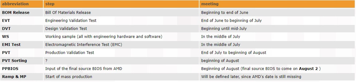
However, it seems that AMD's BIOS is only scheduled to be sent to AIB partners on August 2nd, and AIB partners still have no word on launch dates from AMD, which would hamper their ability to move on to mass production of their designs. This may mean a paper launch from AMD, or perhaps a launch with only AMD reference designs being available for order. Remember that final BIOS is a particularly important part on partner's design customizations, since these usually include info on stock AMD-defined power and temperature limits, power states and fan curve, which partners leverage in building their customized cooling solutions.

https://www.techpowerup.com/235067/...ga-manufacturing-bios-release-schedule-leaked

Paper launch incoming
 
Nah, tile based rasterization is handled on the driver + hardware level. It took some digging by someone very knowledgeable (and clever) to figure out that Maxwell switched to this. It's not even officially acknowledged by Nvidia as far as I remember.

If every developer had to code for it, it would be well documented.


nV talked about it with Pascal. Extensively too.

And now I don't think that is how it works in Vega, cause the way Scott W talked about with Witcher 3 though primitive shaders, doesn't seem to be automatic for them, but they kinda talked about two things there the rasterizer and the improvements to polygon through put, so the could have been just talking about polygon through put, but knowing how Scott tends to be pretty clear when discussing topics like these, I would say both. Well White papers for RX Vega haven't been released yet, so don't know yet.

Had this discussion with Anarchist a while back too. Close to a year ago, AMD is on its first iteration of a tiled rasterizer, nV is on their second and with Volta will be third.

AMD also had to recreate their patent for it cause they sold off their mobile division, so they can't just make the same thing they had before in their mobile chips, hence the use of the primitive shaders, which will give them more flexibility in the long run. We just have to see how it plays out in the short term. The ease of implementation of such a feature, and what happens when primitive shaders emulate the tradition fixed function pipeline.
 
Last edited:
nV talked about it with Pascal. Extensively too.

And now I don't think that is how it works in Vega, cause the way Scott W talked about with Witcher 3 though primitive shaders, doesn't seem to be automatic for them, but they kinda talked about two things there the rasterizer and the improvements to polygon through put, so the could have been just talking about polygon through put, but knowing how Scott tends to be pretty clear when discussing topics like these, I would say both. Well White papers for RX Vega haven't been released yet, so don't know yet.

I think you're confusing tessellation and rasterization and primitive shaders a bit?

 
I think you're confusing tessellation and rasterization and primitive shaders a bit?


NO I'm not lol. check the videos again, I had long discussions with other members in this forum about both tessellation and TBR.

Also have to understand TBR works great for deferred rendering not so good for forward rendering. So AMD's push towards that as well as nV push for that in VR is going to be a problem for a non programmable solution in the future, and this is probably why AMD went this route right now, just so they will be ahead of the game when the time comes when Forward renderers become the fore front of gaming engines.

http://techreport.com/review/31224/the-curtain-comes-up-on-amd-vega-architecture/3

The draw-stream binning rasterizer won't always be the rasterization approach that a Vega GPU will use. Instead, it's meant to complement the existing approaches possible on today's Radeons. AMD says that the DSBR is "highly dynamic and state-based," and that the feature is just another path through the hardware that can be used to improve rendering performance. By using data in a cache-aware fashion and only moving data when it has to, though, AMD thinks that this rasterizer will help performance in situations where the graphics memory (or high-bandwidth cache) becomes a bottleneck, and it'll also save power even when the path to memory isn't saturated.

it really does sound like its programmable dude.
 
Last edited:
NO I'm not lol. check the videos again, I had long discussions with other members in this forum about both tessellation and TBR.

Also have to understand TBR works great for deferred rendering not so good for forward rendering. So AMD's push towards that as well as nV push for that in VR is going to be a problem for a non programmable solution in the future, and this is probably why AMD went this route right now, just so they will be ahead of the game when the time comes when Forward renderers become the fore front of gaming engines.

http://techreport.com/review/31224/the-curtain-comes-up-on-amd-vega-architecture/3


it really does sound like its programmable dude.

I mean, you're wrong according to David Kanter's video and Anandtech's follow up article from last year?

http://www.anandtech.com/show/10536/nvidia-maxwell-tile-rasterization-analysis

http://www.realworldtech.com/tile-based-rasterization-nvidia-gpus/

If developers had to implement these changes in their games (and not in drivers) then why Mr. Kanter have to play detective well after Maxwell's release?

EDIT: From that Techreport article relating to DSBR

To help the DSBR do its thing, AMD is fundamentally altering the availability of Vega's L2 cache to the pixel engine in its shader clusters. In past AMD architectures, memory accesses for textures and pixels were non-coherent operations, requiring lots of data movement for operations like rendering to a texture and then writing that texture out to pixels later in the rendering pipeline. AMD also says this incoherency raised major synchronization and driver-programming challenges.
 
Last edited:
Back
Top