Vega Rumors

lol, no and this is what we get above in the mean time.

Bottom line after all the above chatter is performance in the end using the different api's. If Vega can show some kind of astonishing performance doing DX 12 stuff over Pascal then it is a mute point what each hardware does inside if both are about the same.

They just like to hear themselves talk, long as Vega performs no one will care how it gets it done. We should know next month how it performs and then will hear about what is wrong with Vega and why it could have been better ;)
 
See, this is where you people get confused. Nowhere did I claim, to need proof. I said: "This is why I think there's a major fundamental difference to the HBCC"

It's an opinion. It's not a statement of fact like you guys like to enjoy throwing around.

So settle the frak down.

I think HBCC is useless unless you want to run multiple 4k games on a single Vega at the same time.

If Vega is 16GB, what are you going to do with the other 14GB?
 
I think HBCC is useless unless you want to run multiple 4k games on a single Vega at the same time.

If Vega is 16GB, what are you going to do with the other 14GB?

Who would ever need more than 64kb of RAM?!?!?! /s

I think HBCC will help the most with the lower end cut down versions that may end up as low as 4gb + HBCC memory in the immediate future. 8gb will be borderline in the near future for Ultra settings, increased memory requirements are inevitable.

Being able to address more will probably extend the usefulness of Vega cards just that much further.
 
Well with increased memory usage, still need more shader power and other things, resolutions are still going up too, so more rops needed. talking about 8k rendering, I don't think any of these cards even 2 x MGPU's of today's top end cards will not be enough to handle the pixel amounts.

Its not just one facet of that card that can be increased.
 
Last edited:
err, the problem is not an entire GPU array, its a per SM basis issue. Partitioning is done on a SM basis, and its a static partition for Maxwell.

You are using the wrong words too, what you just described there is concurrency not parallelism, concurrency of kernels in the entire Array is not an issue. Concurrency per SM is an issue with Maxwell, because it has a static partitioning, so once partitioned it must stick to that partition or flush the SM and repartition.

This is what has changed from Maxwell to Pascal, the static partitioning is now dynamic partitioning. No need to flush the SM out anymore to reallocate resources based on needs.

You have no idea what you're talking about.

Quadrant setup? Whole GPU context switch? Is this a random jumble of words?

There you go
JustReason in, posting this for the billionth time in a vain attempt to combat your militant sciolism

Guys, why are you wasting time?. why are you trying to argue with a guy who only CPU and GPU "expertise" comes from gaming hundreds of hours a week. lol.
 
Guys, why are you wasting time?. why are you trying to argue with a guy who only CPU and GPU "expertise" comes from gaming hundreds of hours a week. lol.

Hahaha. That sounds like me. So much of this talk is way way over my head.
 
Well with increased memory usage, still need more shader power and other things, resolutions are still going up too, so more rops needed. talking about 8k rendering, I don't think any of these cards even 2 x MGPU's of today's top end cards will not be enough to handle the pixel amounts.

Its not just one facet of that card that can be increased.

But it's not all resolution based, textures and other assets fit in there too which can be bumped up.
 
While I get HBCC- it reminds me of the original application of AGP, that textures would be 'streamed' across the bus as needed, and was highly featured in Intel's i740 graphics adapter in 8MB framebuffer-only variant, I don't see it as a huge limitation except for HBM implementations where total memory is limited. GDDR5x/6 is cheap enough it seems to be included in sufficient quantities for consumer applications, and professional applications are hardly so sensitive to BOM to limit included VRAM.

So it's cool, and will be interesting to see it work, assuming that it's actually well and broadly implemented.
 
I think HBCC is useless unless you want to run multiple 4k games on a single Vega at the same time.

If Vega is 16GB, what are you going to do with the other 14GB?

Not useful for dGPU, but for APU with 2GB of HBM2 only, could be very useful. It's really a HPC feature that AMD is trying to sell for gaming. But if RX Vega comes with 8GB, that's still more than enough for 4K gaming.
 
Once again, you have made a comparison without point of comparison. That is just a basic fallacy.

And what do you have to compare it with? Did you run the same test on Vega? No? Then why the fuck are you talking about "as compared to"?

Are you pretending to be stupid? Vega can't run that CUDA test. Nor would it be required to demonstrate it's capability to easily handle multi-Terabyte datasets, which it's own demos show a major performance gain.

On the other hand, P100's demo, from NVIDIA themselves, show it tanking badly once dataset exceeds it's VRAM limit.

There's a difference there, it's not exactly subtle.

If that was NV trying to show their best light for folks to interpret, the outcome isn't exactly stellar is it?


First off we don't know Vega's performance when applications go above its frame buffer and addressing from off board memory and how much going over it will do to scaling performance. So to come up with your conclusion that its better than nV's unified memory at this point is kinda moot. Now back to the chart you linked to, its unrealistic data sets, its a torture test, its like loading up a power virus to test oh much juice a GPU consumes and to show that as the GPU's regular use TDP. Is that realistic to you?

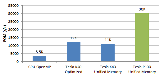
As it right now nVlink provides 30% more performance if I'm reading it right with unified memory when using nvlink, and 5% when using pci-e now if you actually read the paper and linked to other applications that would have been nice, like this one.

lulesh_openacc_with_p100-2.png


You have to understand AMD showed us best case so far with HBCC, this is best case for unified memory ;)
 
First off we don't know Vega's performance when applications go above its frame buffer and addressing from off board memory and how much going over it will do to scaling performance. So to come up with your conclusion that its better than nV's unified memory at this point is kinda moot. Now back to the chart you linked to, its unrealistic data sets, its a torture test, its like loading up a power virus to test oh much juice a GPU consumes and to show that as the GPU's regular use TDP. Is that realistic to you?

As it right now nVlink provides 30% more performance if I'm reading it right with unified memory when using nvlink, and 5% when using pci-e now if you actually read the paper and linked to other applications that would have been nice, like this one.

You have to understand AMD showed us best case so far with HBCC, this is best case for unified memory ;)

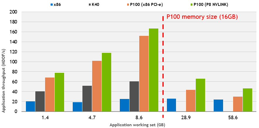
Why is a 58.6GB dataset presented by NVIDIA an unrealistic use case or equivalent of "power virus"? That's not much bigger than the GPU's VRAM, when we put it into context such as 512 TB virtual address space.

Your other example, doesn't list the actual dataset size. Because K40 is actually able to run it, it would therefore be smaller than the Tesla's VRAM limit, so we're talking about a small dataset in that example of "unified memory"... that doesn't even go off it's GPU vram. lol

You do realize pre-GP100, NV's unified memory cannot go beyond the GPU's vram limit, right?

AMD's HBCC demo is very different, it shows fluid performance even with datasets into the multi-Terabyte range, not just 58.6 Gigabytes. Orders of magnitude larger data exceeding the 16GB HBM2.


What nV showed right there in that chart, and yours btw, is that unfied memory with HBM and nvlink works better than unified memory with GDDR type memory with pci-e as the transfer bus. That is SIMILAR but not the same thing AMD showed cause of the nVlink, but when you start looking at the data sets you think 28 gb or 58 GB is realistic, AMD Vega will probably hit the same problem at those crazy amounts right?

You can't compare what AMD showed with HBCC with 4 gb data set vs 2 gb HBM or 8 gb data set vs 4 gb HBM vs what nV showed in those charts. Lets take something like AMD Vega with 8 gb and put it to the test with 16 gb or 32 gb data sets and see what happens. That would be the closest comparative tests we can do to the nv charts.

Now with bandwidth, as data is being transferred, if the data sets aren't crazy amounts, the performance loss shouldn't be there, because the card is being feed quickly but if the bus gets saturated with the transferring data, it doesn't matter, what memory or GPU is there, its screwed.

This is why streaming textures/assets in large scale MMO's have worked, I can't think of a single game that came out in recent years that didn't do it, And its not hard to do, yeah its nice developers don't need to worry about it but really how hard is it to do? Camera position, vs world asset position and keep track of that, and bam its done, streaming assets a go. Developer just have to make sure the art assets don't saturate the bandwidth amounts of a x16 pci-e bus. You can get even more granular with it by having differential algorithm based on distance.

Example, character is locked at point 1.1.1 on the map, then start streaming assets that are a visible distance way from them of 100 meters. Level designers have to be aware of how to set up the levels too based on that distance when streaming starts. Level designers thought process won't change with HBCC either. More granularity can be based on FOV and distance or multiple distances based on locality on the map, indoor vs. outdoor via portal (visareas, depending on the type engine) designations. Or if the engine is using an oct tree or what ever type of data organizational system, plug it into that to figure things out.

Many ways developers have come up with ways of doing it.

Back to bandwidth and data set size, bandwidth to the chip stays the same but if the data set transferring gets to a degree of saturating that bus, there will be a cliff. AMD didn't show us that cliff, they aren't saturating the bus, nV is in those graphs that is why we see the hit.

What AMD showed us was, as long as the data set was in reasonable size, HBCC works, guess what, that works on ALL CARDS, just that programmers don't need to spend extra time in their game engines anymore to do that, they can relay on the HBCC to take care of it.
 
Last edited:
Why is a 58.6GB dataset presented by NVIDIA an unrealistic use case or equivalent of "power virus"? That's not much bigger than the GPU's VRAM, when we put it into context such as 512 TB virtual address space.

Your other example, doesn't list the actual dataset size. Because K40 is actually able to run it, it would therefore be smaller than the Tesla's VRAM limit, so we're talking about a small dataset in that example of "unified memory"... that doesn't even go off it's GPU vram. lol

You do realize pre-GP100, NV's unified memory cannot go beyond the GPU's vram limit, right?

AMD's HBCC demo is very different, it shows fluid performance even with datasets into the multi-Terabyte range, not just 58.6 Gigabytes. Orders of magnitude larger data exceeding the 16GB HBM2.

Honestly, you trust what AMD shows us? When was the last time that worked out?
 
What nV showed right there in that chart, and yours btw, is that unfied memory with HBM and nvlink works better than unified memory with GDDR type memory with pci-e as the transfer bus. That is SIMILAR but not the same thing AMD showed cause of the nVlink, but when you start looking at the data sets you think 28 gb or 58 GB is realistic, AMD Vega will probably hit the same problem at those crazy amounts right?

You can't compare what AMD showed with HBCC with 4 gb data set vs 2 gb HBM or 8 gb data set vs 4 gb HBM vs what nV showed in those charts. Lets take something like AMD Vega with 8 gb and put it to the test with 16 gb or 32 gb data sets and see what happens. That would be the closest comparative tests we can do to the nv charts.

You should look at it again.

unified_memory_oversubscription_hpgmg_perf_no_hints_jan2017.png


P100 is HBM2, there's no GDDR + PCI-e. It's simply P100 + PCI-e (Xeon) or P100 + NVLink (IBM P8).

K40 cannot handle datasets bigger than it's VRAM limit, this is why it failed the workload at 28.9GB.

What NV is demonstrating here, is P100 can handle larger dataset than it's 16GB vram limit (something previous Teslas cannot do), but it will take a major performance hit. NVLink is better because it's faster than PCI-e in bandwidth. What this shows is P100 is limited in performance since it has to wait on data transfers over the bus, and PCI-e is just slow when the dataset gets large.

In context, AMD's demos are not GPU acceleration of 4/8 or even 16/32 GB datasets. It's TeraByte datasets. TERABYTES. Well beyond Vega FE's 16GB HBM2. Ofc, you could argue AMD is probably lying and just making up their demos...

When Volta arrives, with it's NVLink being 2x faster, when it accelerates datasets bigger than it's VRAM limit, I fully expect performance to be much higher than P100 due to the bus bandwidth of NVLink2. And no doubt NV will demonstrate this and show it off too, with maybe 117.2GB datasets instead of 58.6GB. :)


Doesn't work that way man, where you even able to understand how the bus bottleneck works?

Hopefully this explanation simplifies it for you

Take a pipe and pour water into it slowly and measure out the water coming out the other end. then pour faster, then pour water into the pipe at such a speed that the water starts overflowing from the inlet. nV showed what happens when its overflowing and the bottleneck of the bus is now also associated with the read speed of the device the assets are coming from. AMD didn't show that lol.

Now the 1 TB demo thing that was totally different, they are streaming to a HD that is on card that is DIRECTLY connected to the HBC memory, there is no bus in the middle and thus that is why they aren't showing the same thing. Also added to this the data set size of 1 TB not all of it is being transferred at one time, parts of it are, so without knowing how much is transferring....... There is nothing to draw from.

So the data set size that is going over the bus is what is important in the nV tables, AMD hasn't showed that yet. So not sure how you are coming with these conclusions or even presuming you can come up with anything that would be a reasonable train of thought.

Now do you get why those tables are unrealistic? When was the last time you heard 28 or 58 gb over a pci - e bus was necessary, well in this case over nvlink and 12 GB and 42 GB? What AMD showed was a 1 tb file that was being loading up but they didn't say all 1 tb was going over to the GPU at ONCE.
 
Last edited:
Honestly, you trust what AMD shows us? When was the last time that worked out?

It works out IF you're smart enough not to project what they show and realize they don't tell you how things were set up. In fact, when you realize that, you get a bloody good idea of how it's going to behave upon review.
 
It works out IF you're smart enough not to project what they show and realize they don't tell you how things were set up. In fact, when you realize that, you get a bloody good idea of how it's going to behave upon review.


Got weed out the bad and keep the good pretty much to create an educated guess.
 
Got weed out the bad and keep the good pretty much to create an educated guess.

Yeah but the issue here , with Vega, is they've changed a lot of crap to orient it towards specific case use for deep learning. No company does that on their own, someone wants that ... so who wants it and how will those changes relate to the average consumer? I have zero idea. The market isn't what it was six years ago.
 
Yeah but the issue here , with Vega, is they've changed a lot of crap to orient it towards specific case use for deep learning. No company does that on their own, someone wants that ... so who wants it and how will those changes relate to the average consumer? I have zero idea. The market isn't what it was six years ago.


If they don't have software to drive their hardware, the AI thing is really a bust, just read a good article on that

http://www.infoworld.com/article/31...-plan-to-become-a-machine-learning-giant.html

Both pieces, the hardware and the software, matter equally. Both need to be in place for AMD to fight back.

What matters even more for AMD to get a leg up, though, is not beating Nvidia on price, but ensuring its hardware is supported at least as well as Nvidia’s for common machine-learning applications.

What’s likely to be toughest of all for AMD is finding a foothold in the places where GPUs are offered at scale. All the GPUs offered in Amazon Web Services, Azure, and Google Cloud Platform are strictly Nvidia. Demand doesn’t yet support any other scenario. But if the next iteration of machine-learning software becomes that much more GPU-independent, cloud vendors will have one less excuse not to offer Vega or its successors as an option.

Still, any plans AMD has to bootstrap that demand are brave.They’ll take years to get up to speed, because AMD is up against the weight of a world that has for years been Nvidia’s to lose.

The last quote of that article I did, if everyone currently is using nV hardware for AI tasks, why would those developers switch over to RoCm? That is a major problem for AMD, its a long road to change that. And if we look at what these companies are looking for for employees for AI, CUDA is a pretty much a prerequisite. So in College what would kids want to be working on, if they want a job once graduating? That is another headache for AMD. Its not just a long road now, its long and its got a lot of cliffs along the way too.
 
It works out IF you're smart enough not to project what they show and realize they don't tell you how things were set up. In fact, when you realize that, you get a bloody good idea of how it's going to behave upon review.

Yeah but the issue here , with Vega, is they've changed a lot of crap to orient it towards specific case use for deep learning. No company does that on their own, someone wants that ... so who wants it and how will those changes relate to the average consumer? I have zero idea. The market isn't what it was six years ago.

Haha you defeated your own post. So now we're left with shitty AMD marketing tactics and no baseline. :D
 
Haha you defeated your own post. So now we're left with shitty AMD marketing tactics and no baseline. :D

I've admitted several times I'm clueless... how do you defeat clueless exactly?

I'm just pointing out someone wants what they're pitching and it isn't necessarily gaming consumers.

But sure, whatever you say.
 
I've admitted several times I'm clueless... how do you defeat clueless exactly?

I'm just pointing out someone wants what they're pitching and it isn't necessarily gaming consumers.

But sure, whatever you say.

It could just be a struggling company's execs saying, "we need to innovate!" and engineering doing the best they can with half the budget they asked for. Some companies like to think if they build it the industry will change for their method. We've seen that a few times with AMD... and companies I've been with.

Regardless this is one part of Vega I don't really care about. I just chuckle when people use AMD's information as facts.

Meh, it's all bullshit unless it makes profit. No matter where. Maybe these will be ultimate mining cards and they'll sell everyone they can make. Try and buy a competitively priced 580 right now. this two company market sucks farts from dead seagulls.
 
Meh, it's all bullshit unless it makes profit. No matter where. Maybe these will be ultimate mining cards and they'll sell everyone they can make. Try and buy a competitively priced 580 right now. this two company market sucks farts from dead seagulls.


I just got 6 of them @ 250 each :), I'm hoping AMD has to cut the price down on Vega to around 550 or less even at 650 it will still be ok for me, I will replace rx 580s for Vega, since it should increase on the perf/watt, which directly translates to $/watt, It would be one of the best investments ever if I'm going to set up a mining farm lol, where in the world of business can you make your money back in 2 months on initial investment? No where lol. Of course I don't expect to to go past 6 months cause of ethereum changing how they pay, but there will be other coins out there that will pick up once ethereum is gone.
 
Software has long been ATI/AMD's weakness.

This has been true the very minute they got serious about gaming with the first Radeons, and continues to be the case and even a selling point, where their products tend to perform 'better' with time due to optimizations that were not available when products were released.

And when it comes to commercial customers whose needs are beyond graphics, AMD has really fallen flat- CUDA was created and exists not as a method for undercutting or locking out AMD as some have claimed, but rather to meet a need not previously being met, that of providing an interface for Nvidia's compute hardware. It is similar to OpenCL which followed it onto the market, but has been from the start the best way to extract performance from Nvidia cards in a small but lucrative market.

Because AMD hasn't made the effort to produce their own efficient API or ensure that OpenCL can be productively used as thus through support and possibly extensions, they have fallen behind, and now we see Nvidia not producing Quadro and Tesla cards as a bit of an afterthought for their largely gaming-focus products, but rather their product design and cycles being dictated by the needs of their commercial compute customers, with consumer versions essentially being slimmed-down derivations.

For AMD, Vega does appear to have a similar impetus of 'compute first', and maybe they will be able to gain a bit of momentum here and capitalize on it, but as mentioned above, they do have a long way to go.
 
Software has long been ATI/AMD's weakness.

SNIP

For AMD, Vega does appear to have a similar impetus of 'compute first', and maybe they will be able to gain a bit of momentum here and capitalize on it, but as mentioned above, they do have a long way to go.

I agree with you, but I really do believe down the road that OpenCL is easier for ad hoc initiatives, we're seeing it in coin mining and we're starting to see it on operating systems. But as usual with AMD, they think the market will do their work for them or they plan for something that won't come for ten years. Which does them no good at all today. Penny wise, pound foolish.
 
Outside of specific commercial implementations, which are typically used with fairly customized software, I'll agree that CUDA doesn't make much sense- it's just part of what's driving Nvidia's market dominance today.

I'd certainly like to see more prevalent use of OpenCL; next to no one is doing great parallel acceleration, even on Apple, whose last Mac Pro essentially banked on GPU Compute.


It would be nice to have an open API and open systems, but its going to take a long time for that, and AMD has to be the driving force to do it, they can't let other companies do work for them, there is no incentive for other companies, cause they can always use nV products as they are doing now.
 
Are you pretending to be stupid? Vega can't run that CUDA test. Nor would it be required to demonstrate it's capability to easily handle multi-Terabyte datasets, which it's own demos show a major performance gain.

On the other hand, P100's demo, from NVIDIA themselves, show it tanking badly once dataset exceeds it's VRAM limit.

There's a difference there, it's not exactly subtle.

If that was NV trying to show their best light for folks to interpret, the outcome isn't exactly stellar is it?
No, it is you who are wearing the AMD ignoramus mask here. Vega's unified memory was not exactly showed in anything but linear read test from a device wired straight to the GPU.
 
Are you pretending to be stupid? Vega can't run that CUDA test. Nor would it be required to demonstrate it's capability to easily handle multi-Terabyte datasets, which it's own demos show a major performance gain.

On the other hand, P100's demo, from NVIDIA themselves, show it tanking badly once dataset exceeds it's VRAM limit.

There's a difference there, it's not exactly subtle.

If that was NV trying to show their best light for folks to interpret, the outcome isn't exactly stellar is it?
It is 5 datasets associated with the HPGMG AMR model - an actual HPC benchmark implementation that is not just CUDA (this support was added later).
Also as I have to keep telling you it is a brutal oversubscription and the blog left it to deal cope without actually doing the ideal coding/workflow.
The point was to show it could still recover from such action, throughput dropped because it went also from 5 sets to 1 and importantly if understand page faults-migration and these have overheads - especially in the scenario Nvidia created.
The slide on its own is meaningless or can be skewed without its actual context.


BTW how are you going to do cohesive unified memory page migration-fault with the HBCC and its 2-terabyte drive and multiple GPUs with said drive (or worst mixed) in a node with 2-CPUs per node and its system RAM?
I still cannot see how it will be used for actual HPC involving node/s and clusters when one considers that and also the latency variation - especially when one scales out and further compounded by the frameworks-system environment management software used by HPC.
Professional visualisation workstations for sure.
Cheers
 
Last edited:
Are you pretending to be stupid? Vega can't run that CUDA test. Nor would it be required to demonstrate it's capability to easily handle multi-Terabyte datasets, which it's own demos show a major performance gain.

On the other hand, P100's demo, from NVIDIA themselves, show it tanking badly once dataset exceeds it's VRAM limit.

There's a difference there, it's not exactly subtle.

If that was NV trying to show their best light for folks to interpret, the outcome isn't exactly stellar is it?

It does not need to run CUDA as the HPC benchmark was created primarily to use MPI/OpenMP3, the CUDA support is a secondary version and makes sense as this is designed for broad use in HPC segment.

benchmark used in the Nvidia Blog said:
High Performance Geometric Multigrid (HPGMG-FV) is a benchmark designed to proxy the finite volume based geometric multigrid linear solvers found in adaptive mesh refinement (AMR) based applications like the Low Mach Combustion Code (LMC). HPGMG-FV is being used to conduct computer science (e.g. Top500 benchmarking, programming models, compilers, performance optimization, and auto-tuners), computer architecture, and applied math research.

.....

There are two public versions of HPGMG. Both implement the 4th order (v0.3) solver. The former is MPI+OpenMP3 while the latter adds CUDA support for the key kernels in order to leverage the computing power of NVIDIA's GPUs: hpgmg on bitbucket (HPGMG-FV is in the ./finite-volume/source sub directory) hpgmg-cuda on bitbucket (v0.3 compliant MPI2+OpenMP3+CUDA7 implementation). Please see NVIDIA's Parallel ForAll blog for more details. Instructions A reference MPI+OpenMP implementation of…
https://crd.lbl.gov/departments/computer-science/PAR/research/hpgmg/

So this benchmark is not tied to Nvidia and never was, comes down to how serious AMD is about HPC.
Cheers
 
My point that you sort of just agreed with is that no-one else is using TressFX 3, and like I said probably because to make it work well one has to have PureHair or equivalent and this was created by the same studio that was heavily involved with TressFX from the early days all the way through to current version.
You mention AMD has put the onus on the devs/studios for this and fits my point, the only studio to successfully implement this in any meaningful way were involved with TressFX creation and evolution.
Also Crystal Dynamics implemented more than just hair in RoTR, it influenced the texture of the snow on AMD GPUs.
The point I was getting at is that many devs seem to be refactoring their engines for DX12/Vulkan and we haven't seen much hair as releases have been limited. I wouldn't go as far as saying the onus is on the devs, but creativity is ultimately the responsibility of an artist. The tool just provides a foundation to be expanded upon.

Regarding hardware scheduler.
I think it is too early to say just how Nvidia has implemented this and I doubt it has any similarity to historical implementations whether hw or more recently sw.
Nvidia could had done the scheduler slightly differently with Maxwell and Pascal but it would had impacted the efficiency of the design at the time, here is what Nvidia says on the subject of with regards to Volta:
Part of this can be seen the use of the new Syncwarp() as well being integral to the new arch.
Both Alben and Catanzaro are heavily involved with the direction and development of Nvidia GPUs.
Too early to tell either way if it is HW or SW or hybrid mix - my view is they have not regressed and not entirely convinced we are seeing a hardware scheduler like one may think of in the past as before Kepler.
Cheers
I'd agree we definitely need to know more. That said the Volta blog did roughly lay out the functionality of the MPS(~ACE in AMD terms). The HWS equivalent is still a bit unclear, and that's where it gets a bit more interesting. The thread scheduler and syncwarp() being discussed is a bit ambiguous. It looks like it's within a single kernel, but on the other hand a kernel that diverges immediately into radically different paths could be considered two separate kernels. So the graphics versus compute distribution is still unclear, but it's not applicable to HPC either which was the focus of the blog and V100.

Nvidia has always had hardware scheduling of warps. Scheduling within warps has been relegated to the software stack since the introduction of a fixed latency math pipeline in Kepler. Because it's redundant.
Hardware scheduling IN warps/blocks is a more accurate description.
We're talking about an entirely different level of scheduling here. With async the scheduling concern is the warp/thread block distribution, not the instructions. Thread management versus execution. The execution part has divergence, the threading part does not to put it simply. Further, async behavior is probably better defined as the ability to adapt to changes in real time. That's not something Nvidia hardware is very proficient at, as the scheduling requires known distributions in advance. Reacting to changes as opposed to anticipating them. One of those is based on guesswork of an increasing number of variables.

In that same vein I'm confident you're aware that Pascal doesn't partition within an SM.
That's precisely the problem. The whole point of async and concurrency is to have complementary tasks scheduled together(in addition to prioritization) to better utilize all the execution units. It's basically hyperthreading. The problem with ILP is by definition all threads are doing the same thing. This varies a bit as they won't all be running in lockstep. Hence they all hit the same bottleneck and probably leave some hardware idle. Or they get stuck on one task and can't quickly shift in another.
 
The point I was getting at is that many devs seem to be refactoring their engines for DX12/Vulkan and we haven't seen much hair as releases have been limited. I wouldn't go as far as saying the onus is on the devs, but creativity is ultimately the responsibility of an artist. The tool just provides a foundation to be expanded upon.


I'd agree we definitely need to know more. That said the Volta blog did roughly lay out the functionality of the MPS(~ACE in AMD terms). The HWS equivalent is still a bit unclear, and that's where it gets a bit more interesting. The thread scheduler and syncwarp() being discussed is a bit ambiguous. It looks like it's within a single kernel, but on the other hand a kernel that diverges immediately into radically different paths could be considered two separate kernels. So the graphics versus compute distribution is still unclear, but it's not applicable to HPC either which was the focus of the blog and V100.


Hardware scheduling IN warps/blocks is a more accurate description.
We're talking about an entirely different level of scheduling here. With async the scheduling concern is the warp/thread block distribution, not the instructions. Thread management versus execution. The execution part has divergence, the threading part does not to put it simply. Further, async behavior is probably better defined as the ability to adapt to changes in real time. That's not something Nvidia hardware is very proficient at, as the scheduling requires known distributions in advance. Reacting to changes as opposed to anticipating them. One of those is based on guesswork of an increasing number of variables.


That's precisely the problem. The whole point of async and concurrency is to have complementary tasks scheduled together(in addition to prioritization) to better utilize all the execution units. It's basically hyperthreading. The problem with ILP is by definition all threads are doing the same thing. This varies a bit as they won't all be running in lockstep. Hence they all hit the same bottleneck and probably leave some hardware idle. Or they get stuck on one task and can't quickly shift in another.


Problem is the MPS is not hardware related, its a service, its application specific and can only run on Linux.

https://docs.nvidia.com/deploy/pdf/CUDA_Multi_Process_Service_Overview.pdf

PS its been there since Fermi.
 
The point I was getting at is that many devs seem to be refactoring their engines for DX12/Vulkan and we haven't seen much hair as releases have been limited. I wouldn't go as far as saying the onus is on the devs, but creativity is ultimately the responsibility of an artist. The tool just provides a foundation to be expanded upon.


I'd agree we definitely need to know more. That said the Volta blog did roughly lay out the functionality of the MPS(~ACE in AMD terms). The HWS equivalent is still a bit unclear, and that's where it gets a bit more interesting. The thread scheduler and syncwarp() being discussed is a bit ambiguous. It looks like it's within a single kernel, but on the other hand a kernel that diverges immediately into radically different paths could be considered two separate kernels. So the graphics versus compute distribution is still unclear, but it's not applicable to HPC either which was the focus of the blog and V100.

MPS has nothing to do with ACEs, it operates on an upper level in terms of hierarchy. We are talking about multiple applications using one GPU. This has nothing to do with asynchronous execution of two different kernels.
Hardware scheduling IN warps/blocks is a more accurate description.
We're talking about an entirely different level of scheduling here. With async the scheduling concern is the warp/thread block distribution, not the instructions. Thread management versus execution. The execution part has divergence, the threading part does not to put it simply. Further, async behavior is probably better defined as the ability to adapt to changes in real time. That's not something Nvidia hardware is very proficient at, as the scheduling requires known distributions in advance. Reacting to changes as opposed to anticipating them. One of those is based on guesswork of an increasing number of variables.

The scheduling *required* (past tense) known distributions in advance to be effective, on Maxwell. On Pascal there is no need to accurately estimate execution times and partition the SMs accordingly, If my compute shader has finished while my graphics kernels are still in execution, Pascal will assign those now idle SMs to the graphics pipeline. The NV equivalent of the ACEs would be the GMU and it's 32 hardware queues.
That's precisely the problem. The whole point of async and concurrency is to have complementary tasks scheduled together(in addition to prioritization) to better utilize all the execution units. It's basically hyperthreading. The problem with ILP is by definition all threads are doing the same thing. This varies a bit as they won't all be running in lockstep. Hence they all hit the same bottleneck and probably leave some hardware idle. Or they get stuck on one task and can't quickly shift in another.

I don't see why this is a problem, claiming that this *the* problem neccessarily entails that the SMs were not (and are not) saturated.

Allowing concurrent execution of warps from different pipelines within the SM is clearly not needed to saturate nvidia SMs. If this were not the case then how do you explain Maxwell, Pascal and now surely Volta outperforming GCN in terms of effective performance/theoretical flop ?

See AotS 4K+ Async
 
Back
Top