Possible AMD Radeon RX 490 Performance Numbers Show Up in DX12 AOTS Benchmark – On Par With High-End

Do we know if all Vega arch will use HBM2? Could Vega 11 have been designed to use DDR5(x)? I am pretty sure AMD was committed to HBM this round but they could have had an option in the design to go DDR5 if HBM2 was not available.

Polaris 10 has 2304 shaders, to then jump to 4096 shaders and something higher makes no sense to me. Seems like Vega 11 will be more like 2816 unless they added a few more CU's or less. A dual Polaris card to me sounds stupid for costs, electrical power and performance coming from it. Probably in most games the 1080 would win with much less power needed with a much cheaper cost to make.

The numbers in AOTS could just be an engineering Vega sample - who knows.
 
If going by Polaris's bandwidth needs, Vega needs HBM 2 to compete with the 1070 and 1080, they can't without it they will be bandwidth limited. I think the fastest GDDR5x right now is x12, which is 20% faster than the memory being used on GTX1080, which they need 25% more. Now if they use a larger bus size like 384 bit then they can use GDDR5x but that is going to be a problem with power consumption its going to be using more than 250 watts at the needed bandwidth to sustain gtx1080 performance (no savings in power consumption with GDDR5x, and increased die size due to the on die bus for GDDR5x).
 
Last edited:
Well with AMD going the HBM2 way of thinking will probably imply less time/money spent on optimizing memory bandwidth other then what was done for Polaris.

Now AMD does not need to beat the 1080 per se, just beat the 1070 where the majority of the sells are. Vega 11 with 8GB of DDR5(x) and call it the 490, $399. If performance is 5%-10% better then the 1070 it should be capable of selling well (minus AMD marketing ability). While Vega 10 will need HBM2, Vega 11 may not need it absolutely.
 
You don't have that kind of control over the data man. I'm not even sure why you mention execution context only because that is only applicable to compute and the problem is the graphics execution because the compute execution is usually tied with graphics execution and that causes the problems.


Problem with that is, we have seen AMD's GCN scaling poorly so far as it gets "larger" in die size. So its possible AMD didn't want to go that route, added to that the power consumption of large die size is not going to be 1 to 1 as we can see Fiji, that water cooler was there for a certain reason, try to drop its power consumption as much as possible. What AMD got with Fiji was ~30% the die size from Hawaii with ~30 % more performance at same power consumption or greater (most likely its greater cause the water cooling cuts the chips temps down a lot as much as 50C which means it would directly translate to 50 more watts if not more because of the increased leakage at such a temperature). That was not good for an updated generation of GCN. Even after using HBM which means all that savings from HBM was to no avail. Now with front end changes its possible to see some of those bottlenecks to be relieved, but we can see not all of them are with Polaris because again, P10 vs GP106, P10 needs 25% more bandwidth and 33% raw shader power to keep up with GP106.

That shows GCN from Hawaii/Granada to Fiji, the architecture is maxed out for what it could have provided since the die size (more units) no longer scaled well (scaling was actually poor) with performance. So AMD can't do the same thing they did with Polaris to Vega otherwise rest assured they will come across a similar problem, as we can see the delta between P10 and GP106 is respectably similar to comparative GPU's in GCN vs Maxwell when it comes to bandwidth and raw shader through put.

I totally agree with you. Hoping Vega was designed keeping that shit in mind. Polaris failed hard only because of clocks, otherwise it is a decent chip. Had they been able to hit 1500 on clock we would have been singing atleast some praise.
 
you need a caching system in between the two chips to cover that latency (physical memory and high speed interconnect between the chips) which is not going to happen because cost is the preventative cause.

I would not be surprised if their SSG efforts are not just an industrial solution....
 
its possibly a step towards that, but still would need something faster than a SSD for the speeds that it would need.
 
  • Like
Reactions: N4CR
like this
its possibly a step towards that, but still would need something faster than a SSD for the speeds that it would need.
Still not fast enough eh.. I guess SSG + decent HBM, or some way to have a separate IMC that runs some dedicated HBM, seems like the sort of thing AMD would do. Expensive interposer but could bring some very interesting performance with smaller dies.
 
You don't have that kind of control over the data man. I'm not even sure why you mention execution context only because that is only applicable to compute and the problem is the graphics execution because the compute execution is usually tied with graphics execution and that causes the problems.
Multiple GPUs, multiple contexts. Wouldn't be too unlike partitioning a single GPU to act as multiple. Normally there is only one, but in this case you could have several graphics in addition to compute. Context just being the various cache and state required to execute the kernel. The extent where communication will be required. In the case of graphics one frame to the next should be independent.

The driver should be able to detect and remap the framebuffer as needed. Even if it means masking off the actual address so it appears as the same location for each GPU. Would take some work, but certainly not impossible.

Problem with that is, we have seen AMD's GCN scaling poorly so far as it gets "larger" in die size.
That scaling is largely attributed to the geometry bottleneck. Performance doesn't scale with die size, but it takes less of a hit as resolution increases. In the case of PS4 Pro we know they are continuously improving that capability. Far better with Polaris and the discard, apparently improved further with PS4 Pro, and further with Vega(likely Scorpio) according to that PS4 Pro architect.

Die scaling in regards to clockspeed is typically a curve and not linear. So the ideal frequency for all products is probably down around the 900MHz mark even for Nvidia. If constrained by TDP that should define the largest possible die size for any silicon. Whether that size is practical is another matter. These cards are getting used for more than just consumer graphics, so large efficient dice make sense. Especially for the high end parts. No reason they can't disable parts and upclock others as needed either.

Do we know if all Vega arch will use HBM2? Could Vega 11 have been designed to use DDR5(x)? I am pretty sure AMD was committed to HBM this round but they could have had an option in the design to go DDR5 if HBM2 was not available.
We know there are two Vega designs. We also know those designs will be used on the mid to high tier APUs for the server market. Maybe there are more, but I haven't heard of anything. Stands to reason there will be a mid and high tier product, and unless they will feed them with DDR4 through the Zen socket HBM and an interposer will be required. From that logic it seems likely both Vega designs will be HBM based.

Still not fast enough eh.. I guess SSG + decent HBM, or some way to have a separate IMC that runs some dedicated HBM, seems like the sort of thing AMD would do. Expensive interposer but could bring some very interesting performance with smaller dies.
NVMe controller with a ramdrive seems more likely. Really don't need HBM with that level of bandwidth when constrained by the PCIE bus. SSD works but a hair slow and overkill on capacity. 3D XPoint might work well. Best bet is some sort of ramdrive or secondary memory pool on the card. Wouldn't be difficult to get 32/64/128 GB of extra ram on the video card that way. SODIMMs might offer an expandable option.
 
  • Like
Reactions: N4CR
like this
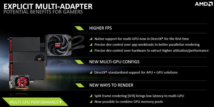
This is very odd but under DX12 you have:
9a570962-927d-4d6c-8e1c-9db7cc2cd3bf.jpg


http://hexus.net/tech/news/software/94249-microsoft-makes-multi-gpu-support-easier-dx12-devs/

So what is this about mGPU is not here yet. Any developer can implement any of the 3 versions of rendering.

The biggest problem is the conflict of interest money wise. A game doesn't sell any more copies for having mGPU. But mGPU support is time, money and resource consuming. Even BF1 struggles with it today, both for DX11 and DX12.

So while AMD and Nvidia can sell you 1 more GPU (incentive), the developer gets absolutely nothing. So in reality the IHVs needs to sponsor games for mGPU support. And that's a death path. Specially since complexity is multifold higher.
 
Something I've been wondering. While mGPU does not have much a future in normal games (at least to me), if there a possibility that VR will be a place for mGPU to shine? Or can single GPUs still power the VR front in the future, especially as graphics still rise on that front?
 
Something I've been wondering. While mGPU does not have much a future in normal games (at least to me), if there a possibility that VR will be a place for mGPU to shine? Or can single GPUs still power the VR front in the future, especially as graphics still rise on that front?

There are new technology types that lowers the difference between single and dual. See Nvidia for example. And then there is other technologies on the way to reduce the graphics need as well.

But then there is the question on why you want 2 high end cards just for VR and a limited benefit. Its clear from Nvidia that they are scaling down on the mGPU front. And I would be surprised if AMD doesn't begin on that as well, if not already. Tho they are still interested in it due to needing 2 cards to compete with 1. But that itself conflicts with the usage pattern for mGPU.
 
Point I was making is that 4096 cores isn't what I would call "huge". Scaling from Polaris I'd expect 4096 cores to be ~400mm2, probably a bit under. Huge would be fiji, P100, GP102 up approaching 600mm2. For a high performance server with HBM2 I'd expect the "big" Vega to be pushing the limits. My working theory is sizing both Vega variants to be less than half the maximum area they can fit on an interposer with the highest SKU being two dice on an interposer. That may yield a ~800mm2 monster alongside HBM2. The limit would seemingly be how big they can make an interposer and the power limit of all the dice at optimal (900MHz?) clocks. Sure you could OC it and push a killowatt, but for a datacenter that would be an ideal chip with the best perf/watt. For an APU just take a GPU and pair with a CPU. The chip in the AOTS results seems more likely to be the small Vega than the large one if not dual Polaris. Also the duel big Vega design as a possibility. That would indeed be a monster.


Data doesn't need to be localized as much as execution context. Keeping the cache and framebuffer localized would be the major concern. Linked adapter changes the current implementations as moving data becomes doable. Low res textures could be duplicated, high res dispersed. The framebuffers and ROPs would be the real bandwidth killer and keeping those local is manageable. It's really just a matter of making sure resources are fully rendered prior to reading them with the other GPU. The task for which barriers were designed. Previous implementations either lack the bandwidth across PCIE (excluding dual cards) and the memory management (SSG flat pool) to properly pull it off. Then properly robust scheduling hardware and appropriate drivers. Even if stalling upon trying to reference output from the other device a good portion of the frame is likely complete. That should be the worse case scenario limiting you to simple pipelined rendering. This is still excluding the explicit methods where a dev designs for two cards.
Yeah,
I guess we see it different because the 4096 core will be on around 500mm2 as that is the cut down release on that die, the full version on the die will be around 15-25% more cores, IMO anyway.
Historically Fiji has a comparable die size to Nvidia larger die.
GP102 for TitanXP or even 1080ti will be 471mm2, GCN is pretty close and comparable to Nvidia part and will be around 470mm2 - 500mm2 (Polaris 480 suggests they are slightly large die design relative to the Pascal part) - that is oversimplifying it but considering they need to overcome previous backend bottlenecks on Fiji and all data on evolution-size of both Maxwell-to-Pascal and Fiji this seems about right.
Hence why 4096 cut down is small Vega IMO and the full release using all the large die is big Vega.
It cannot be any smaller than this because it is competing not just at the upper end of PC Gaming but against P100 and importantly GP102 Tesla cards, yeah I get you think they will only use smaller dual Vega dies per card in HPC-Deep Learning-analytics to compete with Nvidia Tesla Pascal and will be interesting to see how this unfolds.
I appreciate one could debate whether around 470-500mm2 can be considered a large die, but IMO it can seen 'sort of' we see with Nvidia and the delay they had in releasing a full uncut version of GP102 on 471mm2, factors obviously as node shrinks silicon-electrical related GPU designs challenge increases (many EE papers out there on this) as also with yield .
It is probably about the limit on the decision for AMD strategy whether to go smaller Vega dual dies or a single large-ish die.
I personally see they will have single cut 1st/single full some time later/ dual GPU launched at some point, all based upon the larger die and some released in both gaming PC sector and HPC-Pro world, but your point has a lot of weight although critically their profit margin is going to be hammered with a dual version as the P100 is now reasonably priced while the P40 is yet to slowly come down.

And yeah I am not convinced yet those AoTS are actually Vega results and could be a 390x replacement dual Polaris.

Edit:
Only P100 is 600mm2, which is interesting when you consider the P40 on 471mm2 actually has greater FP32 TFLOPs - yeah no fp16/fp32 mixed precision or fp64 CUDA core or support for NVLink.

Size history:
980ti: 601mm2
TitanXP: 471mm2
980: 398mm2
1080: 314mm2
960: 228mm2
1060: 200mm2

FuryX: 596mm2
480: 228m2 but tricky to compare to like for like previous AMD gen for size, gives indicator with 1060 though.

Cheers
 
Last edited:
But mGPU support is time, money and resource consuming.

That's what people said about Mantle/DX12/Vulkan can't do it to much money to much time and we all know how it ended. Ends up smart developers using it in their engine. The rest of what you uttered was just pure nonsense ...
 
That's what people said about Mantle/DX12/Vulkan can't do it to much money to much time and we all know how it ended. Ends up smart developers using it in their engine. The rest of what you uttered was just pure nonsense ...

You mean sponsorship deals or Microsoft titles. That's correct.

And we all seen the glorious success of DX12 so far. Oh the irony!
 
Multiple GPUs, multiple contexts. Wouldn't be too unlike partitioning a single GPU to act as multiple. Normally there is only one, but in this case you could have several graphics in addition to compute. Context just being the various cache and state required to execute the kernel. The extent where communication will be required. In the case of graphics one frame to the next should be independent.

The driver should be able to detect and remap the framebuffer as needed. Even if it means masking off the actual address so it appears as the same location for each GPU. Would take some work, but certainly not impossible.

Its never that simple ;) if its that simple, they would have done it already, this is what I have been saying all along right? But it can't be done right now because its not that simple.

That scaling is largely attributed to the geometry bottleneck. Performance doesn't scale with die size, but it takes less of a hit as resolution increases. In the case of PS4 Pro we know they are continuously improving that capability. Far better with Polaris and the discard, apparently improved further with PS4 Pro, and further with Vega(likely Scorpio) according to that PS4 Pro architect.

Die scaling in regards to clockspeed is typically a curve and not linear. So the ideal frequency for all products is probably down around the 900MHz mark even for Nvidia. If constrained by TDP that should define the largest possible die size for any silicon. Whether that size is practical is another matter. These cards are getting used for more than just consumer graphics, so large efficient dice make sense. Especially for the high end parts. No reason they can't disable parts and upclock others as needed either.

Then why does P10 with 25% more bandwidth and 33% more shader horsepower around the 1060 then?

Simple they haven't fixed it enough or there are other areas where they are bottlenecked.
 
That's what people said about Mantle/DX12/Vulkan can't do it to much money to much time and we all know how it ended. Ends up smart developers using it in their engine. The rest of what you uttered was just pure nonsense ...


And have we seen many successful LLAPI implementation, outside of 4, all others have been pretty bad......
 
Regarding Vega and separate to the AoTS result,
how solid was the number of sources pertaining to it having 12TFLOPs FP32?
If this is actually true (and a massive IF as I am not aware of multiple solid sources I would rely on myself) then that suggests it cannot be small die 2x4096 cores, while a single 4096 Vega core would not hit 12TFLOPs, but a 25% increased core count and associated increase of transistors and some clocks on a larger die could (context fitting with my posts earlier).
The data sort of aligns looking at the Maxwell M40 (7TFLOPs) to Pascal P40 (has 12 TFLOPs), allowing for 25% increase in cores and also the clock speed increase.
Fiji would not need as great a clock increase as it would be coming from around 8.5TFLOPs.

Just raising this as it has implications on the thread, countering that the AoTS results could fit a marginal improved 4096 Vega core/single small die (marginal performance gain relative to same tier Pascal for greater efficiency/thermals) and why no longer competes with higher than 1080 (would need dual die then to compete with and beat in certain configuration Nvidia's higher offerings until they do a dual release or Volta themselves) - not saying this is my view as it has implications on time to market-logistics-price but worth thinking about as does fit explanation from some others.
Depending upon game it would fit anywhere below 1080 to equal in single die release, but becomes quite costly when looking at releasing various cut cores in a dual version to meet various price and tier ranges.
The competition and tier changes subtly when implemented for HPC-deep learning-analytics.

Cheers
 
Last edited:
The biggest problem is the conflict of interest money wise. A game doesn't sell any more copies for having mGPU. But mGPU support is time, money and resource consuming. Even BF1 struggles with it today, both for DX11 and DX12.

So while AMD and Nvidia can sell you 1 more GPU (incentive), the developer gets absolutely nothing. So in reality the IHVs needs to sponsor games for mGPU support. And that's a death path. Specially since complexity is multifold higher.
Take multi-engine and there is less emphasis on matching GPUs. While increasing framerate is great, that may also be achieved by offloading AI, sound, physics to a second adapter. That shouldn't take a whole lot of work for devs to redirect. For actual framerate the DX12/Vulkan synchronization primitives provide a lot of what would be needed for multi adapter. Expanding the process out for multiple linked adapters shouldn't take a lot of extra work. The driver is provided explicit dependencies on how far it can run ahead and has the ability to schedule around issues with the async.

Something I've been wondering. While mGPU does not have much a future in normal games (at least to me), if there a possibility that VR will be a place for mGPU to shine? Or can single GPUs still power the VR front in the future, especially as graphics still rise on that front?
It's interesting because of caching during the rendering process. Both eyes are generally looking at same areas so there is a lot of efficiency gained from shared data. On the flip side mGPU has a lot more available horsepower. So while one GPU per eye works, a better implementation might be to offload certain tasks to a second adapter to free up the other to focus on something specific.

I personally see they will have single cut 1st/single full some time later/ dual GPU launched at some point, all based upon the larger die and some released in both gaming PC sector and HPC-Pro world, but your point has a lot of weight although critically their profit margin is going to be hammered with a dual version as the P100 is now reasonably priced while the P40 is yet to slowly come down.
I think the dual version could actually help the profit margin. It's a high performance part without all the R&D of a whole new SKU. No new masks, custom layouts, inventory, and likely improved yields from small effective die size. Plus like dice could be paired up to match performance. A lot of the cost is already sunk on the interposer for HBM. Simply adding another chip isn't a huge ask and interposer designs aren't all that complicated. It's definitely an interesting concept to see how it will play out if that's the direction they go.

I appreciate one could debate whether around 470-500mm2 can be considered a large die, but IMO it can seen 'sort of' we see with Nvidia and the delay they had in releasing a full uncut version of GP102 on 471mm2, factors obviously as node shrinks silicon-electrical related GPU designs challenge increases (many EE papers out there on this) as also with yield .
More an argument of yield curves to my mind. Difficult to quantify as the data is closely guarded, but smaller dice are always better. Beyond just smaller die size there are fewer actual designs to streamline inventory and design. Really only possible when an interposer comes into play.

Its never that simple ;) if its that simple, they would have done it already, this is what I have been saying all along right? But it can't be done right now because its not that simple.
Are you that sure it's not already starting to happen? We're only just starting to get the hardware and software in place to pull it off.

If this is actually true (and a massive IF as I am not aware of multiple solid sources I would rely on myself) then that suggests it cannot be small die 2x4096 cores, while a single 4096 Vega core would not hit 12TFLOPs, but a 25% increased core count and associated increase of transistors and some clocks on a larger die could (context fitting with my posts earlier).
Have to be careful how you count those cores. AMD doesn't count their scalars, so the math could get a bit fuzzy.

Keep in mind scaling will have a fixed constant area for a significant portion of the chip. AMDs hardware scheduling and media segments likely consume more space than Nvidia's. So ~50mm2+178mm2(2304 cores). Say 0.08 mm2/core would give 316mm2 + 50mm2 for the fixed area. These are very rough estimates with no evidence to back them up beyond some basic engineering. Might be able to get a better estimate if someone wants to find a die shot and break down the areas by usage.

If that 12TFLOPs is counting that scalar design I was theorizing over at B3D that number is going to be rather flexible and unlikely sustainable. The scalars would increase the size a bit, but likely not appear in the core count as they'd have different speeds etc. That design was more about increasing efficiency than peak throughput, but may actually buy you a couple extra TFLOPs. TFLOPs that won't follow the conventional area math. I just doubt they sustain North of 4GHz for a prolonged period. Take a Fiji, increase clocks around 25% where Polaris sits, and add in a few TFLOPs from added scalars it could hit 12.
 
Are you that sure it's not already starting to happen? We're only just starting to get the hardware and software in place to pull it off.

I know its not happening if it was I would be talking to others about it ;) Same limitations exist that is why its not happening.
 
Have to be careful how you count those cores. AMD doesn't count their scalars, so the math could get a bit fuzzy.

Keep in mind scaling will have a fixed constant area for a significant portion of the chip. AMDs hardware scheduling and media segments likely consume more space than Nvidia's. So ~50mm2+178mm2(2304 cores). Say 0.08 mm2/core would give 316mm2 + 50mm2 for the fixed area. These are very rough estimates with no evidence to back them up beyond some basic engineering. Might be able to get a better estimate if someone wants to find a die shot and break down the areas by usage.

If that 12TFLOPs is counting that scalar design I was theorizing over at B3D that number is going to be rather flexible and unlikely sustainable. The scalars would increase the size a bit, but likely not appear in the core count as they'd have different speeds etc. That design was more about increasing efficiency than peak throughput, but may actually buy you a couple extra TFLOPs. TFLOPs that won't follow the conventional area math. I just doubt they sustain North of 4GHz for a prolonged period. Take a Fiji, increase clocks around 25% where Polaris sits, and add in a few TFLOPs from added scalars it could hit 12.
Not sure I follow, I am basing the AMD core count from Fiji, are you suggesting the 4096 core reports for Vega is not the same 4096 count approach for Fiji?
For scaling we can look somewhat to Polaris and also previous gen and also with Nvidia, like I mentioned I agree it becomes more blurred due to back-end functions on die, and as you say they consume more space which fits with my earlier posts where I mention the size of Polaris 480 vs Pascal 1060 among the other trends with figures as well.
That 12TFLOPs is based upon how the cores were numbered in the past for Fiji, as far as I am aware.
You do agree that AMD increased the CU and in doing so the core count for Polaris 480 in same way Nvidia increased SMM and core count?
They did it for Polaris (close-ish to Tonga), so it should be doable for Vega unless Fiji was at the absolute limit (although Nvidia while capped at 6 GPC like before increased cores at SMM per GPC level architecture change).
Cheers
 
Last edited:
I think the dual version could actually help the profit margin. It's a high performance part without all the R&D of a whole new SKU. No new masks, custom layouts, inventory, and likely improved yields from small effective die size. Plus like dice could be paired up to match performance. A lot of the cost is already sunk on the interposer for HBM. Simply adding another chip isn't a huge ask and interposer designs aren't all that complicated. It's definitely an interesting concept to see how it will play out if that's the direction they go.


More an argument of yield curves to my mind. Difficult to quantify as the data is closely guarded, but smaller dice are always better. Beyond just smaller die size there are fewer actual designs to streamline inventory and design. Really only possible when an interposer comes into play.
Wanted to split this out as it fits more with this thread.
I do not think a dual version card has ever been more economical than a single die version from the manufacturers' perspective even allowing for yields and here we are talking at most a 500mm2 die, though definitely for the buyers.
There is a reason why historically AMD and Nvidia only do the dual card versions for maximum top tier performance and then usually for the HPC-data analytics-Pro world, the lower model S7150x2 is a server focused card and its price retail is 67% higher than the S7150 (which is not really a cheap card itself) - basing this on the standard x2 and not reverse airflow.
If AMD has managed to make this work and with good profit margins that would be very good, but the general rule is its margins will be tighter unless they charge much more for it compared to a close to performing single GPU card.
And one primary factor in logistics (not the only logistical variable) is that you need double the number of GPUs for manufacturing/launch.

Cheers
 
Last edited:
Not sure I follow, I am basing the AMD core count from Fiji, are you suggesting the 4096 core reports for Vega is not the same 4096 count approach for Fiji?
Yes, if they are doing what I think. The scalars aren't counted for Fiji with 1 scalar per CU. So they don't show in core count or FLOPs. My theorized design has 4 scalars at 4x (somewhat arbitrary) clocks per CU. A 4096 core design like Fiji would therefore have the equivalent of 1024 cores that weren't counted. Again I'm speculating here, but such a design would definitely change the math.

You do agree that AMD increased the CU and in doing so the core count for Polaris 480 in same way Nvidia increased SMM and core count?
In general yes, but the scalar processors may make it interesting as they aren't counted.

They did it for Polaris (close-ish to Tonga), so it should be doable for Vega unless Fiji was at the absolute limit (although Nvidia while capped at 6 GPC like before increased cores at SMM per GPC level architecture change).
Fiji had entire sections whacked off to make it fit within the 600mm2 windows with the HBM. Fiji was definitely at the absolute limit of the design as the 20nm process fell through. The CUs were likely intact, but front end a mess. Again it's the scalar counting that throws off the math. As for Polaris I think the CU count was adjusted downward towards available memory bandwidth.

I do not think a dual version card has ever been more economical than a single die version from the manufacturers' perspective even allowing for yields and here we are talking at most a 500mm2 die, though definitely for the buyers.
I have no evidence to back this up beyond assuming reusing existing components is more cost effective than creating new ones. Board design and components being a relatively insignificant portion of the overall development costs compared to a significantly large chip with limited volume.

If AMD has managed to make this work and with good profit margins that would be very good, but the general rule is its margins will be tighter unless they charge much more for it compared to a close to performing single GPU card.
And one primary factor in logistics (not the only logistical variable) is that you need double the number of GPUs for manufacturing/launch.
Margins might be lower, but there's a lot of other costs that would go into the design that the margins won't take into account. Essentially it removes all R&D costs save for the board design. Yes you need double the GPUs for the design, but you're reusing the same cores for your mid to high tier product. You could also choose to bin out of that same pool. A far larger pool should benefit binning and it's almost guaranteed to sell more mid to high tier products than enthusiast class.
 
  • Like
Reactions: N4CR
like this
Yes, if they are doing what I think. The scalars aren't counted for Fiji with 1 scalar per CU. So they don't show in core count or FLOPs. My theorized design has 4 scalars at 4x (somewhat arbitrary) clocks per CU. A 4096 core design like Fiji would therefore have the equivalent of 1024 cores that weren't counted. Again I'm speculating here, but such a design would definitely change the math.

They won't change their shader array off of what they have in the consoles, it will cause a lot more work for their driver team, actually it will divide their driver team to work on two separate projects


Fiji had entire sections whacked off to make it fit within the 600mm2 windows with the HBM. Fiji was definitely at the absolute limit of the design as the 20nm process fell through. The CUs were likely intact, but front end a mess. Again it's the scalar counting that throws off the math. As for Polaris I think the CU count was adjusted downward towards available memory bandwidth.


And this is why they can't do that this time, cause if they do, its going to make the same problem Fiji had. I would not be surprised if Vega ends up at GP102 size.
 
They won't change their shader array off of what they have in the consoles, it will cause a lot more work for their driver team, actually it will divide their driver team to work on two separate projects
That change should be largely transparent to drivers though. It would be like having more SIMDs to schedule against which doesn't necessarily change the code that gets written. SIMD scheduling is a hardware driven feature. Waves just executes a bit more quickly or efficiently. Opens up some new options for new instructions, but existing code still works fine. Big question would be if fixed function geometry got moved into the CUs. No idea on the accuracy, but some leaked diagrams suggest it might actually be in a console design.
 
I might be confused at what you are saying, can you give me more details?
 
I might be confused at what you are saying, can you give me more details?
The change I was proposing at the simplest level would just adjust the SIMD execution. They would still be 16 wide SIMD with the decode logic determining which wave was executed. That should be entirely transparent even to the driver. A wave would be dispatched to a SIMD and it would proceed to execute all assigned waves according to it's own scheduling logic. Looping through waves as they become ready. Think of my scalar proposal as 1 wide vector SIMD alongside the typical SIMD. You wouldn't have to utilize it, but the logic could put two ready waves in flight simultaneously, albeit starting at different times. The scalar unit would be a bit strange with a temporal aspect to it. So the scheduler would pass it the operands over 4 cycles and read the value out sometime in the future when it completed and issued the next instruction. Think of the scalar for looping through a vector in the background while the SIMD worked normally. When the scalar finished the SIMD would idle while more work was scheduled. So cycles 0-3 the scalar is decoding a single instruction, cycles 4-15 the SIMD executed 3 instructions. As a scalar isn't performing 16 instructions within 4 cycles, both the scalar and SIMD are in theory executing at the same time for a performance gain. At a high level you're still working on waves of 16x4, just far more efficiently for certain workloads. There are a whole host of ways that could be set up and I'm speculating on the implementation here. Lots of ways that could be improved, but keeping it simple here.

As for the diagram, what I recall was replacing an entire SIMD with a set of scalars. Different than my theory and seemingly a bit more limited as waves don't migrate SIMDs. It could be tailored towards a smaller effective wave size though. Works for partial waves at the start, but not diverging workloads unless AMD developed a migration capability. Not sure it was an actual design document or someone's interpretation. It was 3 SIMDs and 4 scalars comprising a CU. Effectively a pack of scalars taking the place of a single SIMD.
 
Ok yeah I know what you are talking about it was a AMD patent. Well drivers, specifically the shader compiler will have to be different, which I don't think AMD will do. Hardware scheduling wise isn't a problem, how you feed the GPU trough the driver/cpu will change though.
 
Ok yeah I know what you are talking about it was a AMD patent. Well drivers, specifically the shader compiler will have to be different, which I don't think AMD will do. Hardware scheduling wise isn't a problem, how you feed the GPU trough the driver/cpu will change though.
It would change if adding features, but if simply processing vector instructions nothing would change. There would be no real performance gain until you started building on that capability by adding more complex instructions, independent scalar workloads, or allowing a dual issue through free operands. That wasn't in the AMD patent, but some of the capabilities originate from there.
 
It will be interesting to see where Vega lands. I personally think it will probably be somewhere in around the GTX 1080, if the rumored core counts are correct, and this is right around that sort of performance. I can't see AMD bringing out another dual-GPU card unless it's the top of the line. They're very expensive to build so unless it's the absolute top tier card they won't be able to sell it at a competitive price.
 
https://www.tonymacx86.com/threads/...d-radeon-drivers.197273/page-118#post-1386344

Going off this in some mac drivers, there's a Polaris 12 and Polaris 10XT2 in addition to the known chips and Vega 10.

that will be one hella of a thing if they got refreshed polaris at higher clock and with little more shaders kicking it. O well we should see. Looks like they might be laucnhing something in december at the event.

Polaris XT and then Polaris XT2 sounds alot like a refreshed version.
 
that will be one hella of a thing if they got refreshed polaris at higher clock and with little more shaders kicking it. O well we should see. Looks like they might be laucnhing something in december at the event.

Polaris XT and then Polaris XT2 sounds alot like a refreshed version.
I imagine lots of people would be thoroughly pissed off if AMD refreshed Polaris this soon.
 
I imagine lots of people would be thoroughly pissed off if AMD refreshed Polaris this soon.

Doesn't stop a company from releasing a better product. What is if it's like ghz edition with much faster clock speeds and little more shaders to go on too.

Wouldn't hurt anyone. But I doubt that's the case. We will see.
 
The change I was proposing at the simplest level would just adjust the SIMD execution. They would still be 16 wide SIMD with the decode logic determining which wave was executed. That should be entirely transparent even to the driver. A wave would be dispatched to a SIMD and it would proceed to execute all assigned waves according to it's own scheduling logic. Looping through waves as they become ready. Think of my scalar proposal as 1 wide vector SIMD alongside the typical SIMD. You wouldn't have to utilize it, but the logic could put two ready waves in flight simultaneously, albeit starting at different times. The scalar unit would be a bit strange with a temporal aspect to it. So the scheduler would pass it the operands over 4 cycles and read the value out sometime in the future when it completed and issued the next instruction. Think of the scalar for looping through a vector in the background while the SIMD worked normally. When the scalar finished the SIMD would idle while more work was scheduled. So cycles 0-3 the scalar is decoding a single instruction, cycles 4-15 the SIMD executed 3 instructions. As a scalar isn't performing 16 instructions within 4 cycles, both the scalar and SIMD are in theory executing at the same time for a performance gain. At a high level you're still working on waves of 16x4, just far more efficiently for certain workloads. There are a whole host of ways that could be set up and I'm speculating on the implementation here. Lots of ways that could be improved, but keeping it simple here.

As for the diagram, what I recall was replacing an entire SIMD with a set of scalars. Different than my theory and seemingly a bit more limited as waves don't migrate SIMDs. It could be tailored towards a smaller effective wave size though. Works for partial waves at the start, but not diverging workloads unless AMD developed a migration capability. Not sure it was an actual design document or someone's interpretation. It was 3 SIMDs and 4 scalars comprising a CU. Effectively a pack of scalars taking the place of a single SIMD.
Problem is we do not really know the performance benefits/cons this has over the existing architecture with its ratio shader engine-Geometry Processor//CU/scalar-cores (4x16 vector units plus 1 scalar unit compared to the possibility of 4x16 vector units plus 4 scalar units).
It sounds nice in theory but how it pans out would need to be seen and whether that approach would be possible to get the most out of it in majority of situations and various operations, or whether it makes sense to keep as is and increase traditional approach.
Still not sure if this can be truly transparent in all operations, and it still would need a lot of finesse on points Razor mentions IMO, along with any possible implications for the microcode.
But not too long to wait (still assuming mid-late Q1 2017 here) and know either way though.
Cheers
 
Last edited:
Problem is we do not really know the performance benefits/cons this has over the existing architecture with its ratio shader engine-Geometry Processor//CU/scalar-cores (4x16 vector units plus 1 scalar unit compared to the possibility of 4x16 vector units plus 4 scalar units).
It sounds nice in theory but how it pans out would need to be seen and whether that approach would be possible to get the most out of it in majority of situations and various operations, or whether it makes sense to keep as is and increase traditional approach.
Still not sure if this can be truly transparent in all operations, and it still would need a lot of finesse on points Razor mentions IMO, along with any possible implications for the microcode.
But not too long to wait (still assuming mid-late Q1 2017 here) and know either way though.
Cheers
Without knowing the specific implementation it would be extremely difficult to model. Peak TFLOPs are easy to calculate, but realistic numbers far more difficult. For the traditional scaling certain obscure instructions could be limited to the scalar. Scalar logic taking a 1/16th of the area of a 16 wide SIMD with the same functionality. Required instructions can be easily supported without bloating the SIMD for rarely used logic. In fact it may actually make the CUs smaller by transitioning rarely used instructions. Have the SIMDs only running MADD, MUL, DP, while scalar is a superset. Would also increase the execution capacity without requiring all the added crossbars. Another expensive component that complicates the design.

SIMD scheduling should be transparent. The compiler has minimal control over the order a wave becomes ready for execution. The scheduling adapts to the latency of assigned waves. Execution rate of certain instructions already changes a bit on architecture. Take FP16 or FP64 performance for example. They aren't going to be double/half rate on all architectures and the compiler won't change much.

Regardless it will be interesting to see which route they went.
 
Although most of that sounds feasible

SIMD scheduling should be transparent. The compiler has minimal control over the order a wave becomes ready for execution. The scheduling adapts to the latency of assigned waves. Execution rate of certain instructions already changes a bit on architecture. Take FP16 or FP64 performance for example. They aren't going to be double/half rate on all architectures and the compiler won't change much.

The compiler/code has a fair amount of control over the order a wave is being executed this is why its important to limit latency as much as possible in code, this is an optimization step shader programmers take to ensure stalls don't happen.

As smart as GPU's/scheduling is getting, its always better to actually fix the issues in code rather than the driver or GPU take care of them because otherwise you might get undesirable results.
 
There is control through various barriers and synchronization, but it's also nearly impossible to account for any collisions that throw a wrench into the gears. The traditional GCN SIMD is just doing a round robin through it's 10(?) waves. There appears to be some prioritization capability in there as well, but if a wave isn't ready it will be skipped. I recall metrics for wave priority and a TTL. So while a programmer could work to limit stalls, the hardware will do it in realtime easily enough. Far simpler with async behavior if you have no idea what the other waves are doing.
 
Without knowing the specific implementation it would be extremely difficult to model. Peak TFLOPs are easy to calculate, but realistic numbers far more difficult. For the traditional scaling certain obscure instructions could be limited to the scalar. Scalar logic taking a 1/16th of the area of a 16 wide SIMD with the same functionality. Required instructions can be easily supported without bloating the SIMD for rarely used logic. In fact it may actually make the CUs smaller by transitioning rarely used instructions. Have the SIMDs only running MADD, MUL, DP, while scalar is a superset. Would also increase the execution capacity without requiring all the added crossbars. Another expensive component that complicates the design.

SIMD scheduling should be transparent. The compiler has minimal control over the order a wave becomes ready for execution. The scheduling adapts to the latency of assigned waves. Execution rate of certain instructions already changes a bit on architecture. Take FP16 or FP64 performance for example. They aren't going to be double/half rate on all architectures and the compiler won't change much.

Regardless it will be interesting to see which route they went.

You had any detailed information on the upcoming Radeon Chill, this seems to be managing the GPU Queue and latency while controlling fps all in terms of reduced power demand and improved dropped frames-latency.
This may impact the intent of your revised model, not had a chance myself to look closely at what latest Chill is doing but it is pretty intrusive and so far game dependent-verified by AMD while also currently only pre DX12 (I think).
Cheers
 
Last edited:
i can't see how nvidia can be faster than AMD in new upcoming games.
 
Back
Top