Thanks a lot for the photo's already spotted some stuff
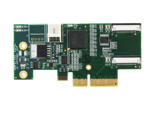
1) 99% sure it's a PLX chip under the heatsink, you can see all traces go from the PCIe finger to the chip and then from the chip to both PCIe slots.
2) On the same PCB you can find a ICS 9DB883AGILF, which is a bigger brother of the IDT 9DB233 I had selected, so good news
Can I request 4 more photos?
a closeup shot of the Chip on the other 2 cards, they are probably the same, on one I can identify the same logo.
And a photo of the back side.
You can see the reference clock signal go upto the first PCIe slot, halfway to the second slot then go into a via, it is probably on the way to the chip on the top left.
Here's a quick collage of my findings

Edit;
First
Damn you [H] for not saving drafts!!!!!
Second
I've been taking a look at both the 9DB833 and the 9DB233 and trying to figure out what the differences are and why the 833 is used.
833 has
Up to 8 Differential Clock signals available
Each signal can be disabled if nothing is connect, so you could run 1 card in a 2 card riser, I'm not sure what the problem might be if you kept the not used signal on, maybe some weird noise?
More control lines to allow finer adjustments
It seems more like an inventory choice, better have 1 slightly more expensive chip you can use in multiple PCBs and the same control logic then using the right chip for that specific application.
All in all I feel like using the 9DB233 should be fine, I just need more information about how to hook it up, I'm not that big in electronics.
1) 99% sure it's a PLX chip under the heatsink, you can see all traces go from the PCIe finger to the chip and then from the chip to both PCIe slots.
2) On the same PCB you can find a ICS 9DB883AGILF, which is a bigger brother of the IDT 9DB233 I had selected, so good news
Can I request 4 more photos?
a closeup shot of the Chip on the other 2 cards, they are probably the same, on one I can identify the same logo.
And a photo of the back side.
You can see the reference clock signal go upto the first PCIe slot, halfway to the second slot then go into a via, it is probably on the way to the chip on the top left.
Here's a quick collage of my findings
Edit;
First
Damn you [H] for not saving drafts!!!!!
Second
I've been taking a look at both the 9DB833 and the 9DB233 and trying to figure out what the differences are and why the 833 is used.
833 has
Up to 8 Differential Clock signals available
Each signal can be disabled if nothing is connect, so you could run 1 card in a 2 card riser, I'm not sure what the problem might be if you kept the not used signal on, maybe some weird noise?
More control lines to allow finer adjustments
It seems more like an inventory choice, better have 1 slightly more expensive chip you can use in multiple PCBs and the same control logic then using the right chip for that specific application.
All in all I feel like using the 9DB233 should be fine, I just need more information about how to hook it up, I'm not that big in electronics.
Last edited: