NVIDIA White Paper Details Multi-Chip Module GPU Design

Logically it isn't much different. You have independent units, with independent memory pools, with interconnects between them.

The devil is in the details. While NUMA is suitable for CPU use, it really isn't for Graphics. This paper isn't really about graphics at all.

Why do you think the memory pool are independent? Just because there is a direct link to a particular pool doesn't mean there isn't mechanisms in place to allow cross talk. There are unique memory architectures which allow for concurrent access for reads.

Snowdog, I think you have tunnel vision.
 
Why do you think the memory pool are independent? Just because there is a direct link to a particular pool doesn't mean there isn't mechanisms in place to allow cross talk. There are unique memory architectures which allow for concurrent access for reads.

Snowdog, I think you have tunnel vision.

Read the paper.

They are independent memory pools with crossbar interconnects if they have to get something from another pool. The big emphasis of the paper is tuning to avoid going across the interconnects because it is so much more expensive.
 
Read the paper.

They are independent memory pools with crossbar interconnects if they have to get something from another pool. The big emphasis of the paper is tuning to avoid going across the interconnects because it is so much more expensive.

With crossfire and sli memory was pretty much duplicated between GPUs. This memory will NOT be segmented in a similar manner where large sections of it are duplicated. Yes they are dedicated to GPU, but the interconnects allow communication.
 
With crossfire and sli memory was pretty much duplicated between GPUs. This memory will NOT be segmented in a similar manner where large sections of it are duplicated. Yes they are dedicated to GPU, but the interconnects allow communication.

Again, RTFP.

The are avoiding the interconnects at all costs for compute loads, Graphics loads are MUCH higher and out of the question.

Maybe some future fantasy tech can share the memory at reasonable speed graphics, but this isn't it.
 
Again, RTFP.

The are avoiding the interconnects at all costs for compute loads, Graphics loads are MUCH higher and out of the question.

Maybe some future fantasy tech can share the memory at reasonable speed graphics, but this isn't it.

I did read the freaking paper. And I'm more than aware of the issues thank you. There are solutions here an intelligent scheduler plus cache can solve.

You're acting like the sub processor will need access to all the memory. If a sub processor is directed to render to a 32x32 sub tile how much texel memory do you think it will need if a scheduler knows ahead of time what triangles are in that tile?

The trick is in the scheduler and cache mechanisms. Setting up the viewing windows and binning the triangles Mapping T3 world space to T2 spaces actually a fairly cheap process. Setting up the draw calls used to be an expensive endevor, but not anymore when it's turned over to the gpu.

It's where you start applying things like z buffer overdraws and alphas and shaders and tesselation advanced filtering and anti alaising and post processing effects and such that things start to get expensive.

Cache and crossbar will play a role when we say "oh yeah I'm a block in the upper left and I need access to data from lower right tile". This is most common in post effect filters like a gaussian blur that needs a surrounding neighbors data.

There are ways around this also. Prefetch and predictive branch loaders can tell you ahead of time if you are going to need cross boundary access and you can preload.

Yeah branch prediction isn't perfect but it is effective. And I'm more than sure both amd and Nvidia have enough data from today's games to be able to determine if they can successfully precache or not and tune that algorithm as necessary.
 
You are just guessing that could work.

If the above were the case, GPUs wouldn't need massive 8-12 GB memory we see currently for gaming cards. That kind of granularity doesn't currently work.

And again this paper is about compute loads as they are much more manageable to localize.
 
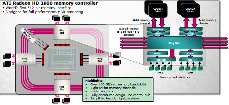
Although not MCM strictly speaking, but AMD was a bit ahead of the curve for no reason as per usual. Shared memory design from R600. Ring-Bus memory for the lulz from a decade ago:

memory_b.jpg
 
Although not MCM strictly speaking, but AMD was a bit ahead of the curve for no reason as per usual. Shared memory design from R600. Ring-Bus memory for the lulz from a decade ago:

memory_b.jpg
I predicted the same approach

If you read the footnotes of research you see a lot of references to interposers and schedulers. It's a lot of what I was talking about before this paper.

They also highlight a lot of the same design challenges and benefits to said architecture the same as me.

If you don't believe me do a search for digitagriffin as poster and navi
 
Last edited by a moderator:
All kidding aside, this ought to help a lot with yields as you can now make a lot smaller chips and when you do, you lose a lot fewer to yields.

To be successful though, those interconnects are going to have to be damned fast.
 
I do wonder what the balance is for throughput vs latency in something like this.
 
Compute, not gaming.

If you expect this for gaming you may end up very disappointed.
 
The way I think of it is this way.

This is not SLI/Crossfire.

1499372839x4vgcn6j2r_1_1.jpg


This is essentially breaking out the subparts that currently exist on a single chip into multiple chips.

A GPU already consists of many hundreds to thousands of little parallel cores. If you can get the interconnects to work fast enough, there should be no reason you can split those thousands of little cores up between multiple chips, and break the non-core related parts out to a separate control chip, called "SYS+I/O" above.

What is the benefit of this? Well, yields go up. The fewer cores you have on the same chip, the higher your yields are, thus costs go down. Also, it might be easier to keep multiple chips separated from eachother cool, than it is to cool all those thousands of cores all in one monolithic chip.

The biggest design challenge here is almost certainly going to be the speed of the interconnects. You'll need the separate chips to be able to communicate as fast with eachother as if they resided on the same die, which is no small feat.

As some as said, this is likely not a gaming design, at least not at first. This is probably going to go into some high end Tesla solution. But who knows, maybe down the road if they can sink the interconnect latencies down far enough, they might actually be able to make gaming cards out of it as well.

Another challenge for gaming is putting all the graphics load balancing logic in the package itself, so you not need CF/SLI drivers. This needs to appear just like a single monolithic GPU to the OS. This is non-trivial IMO given all the issues with SLI/CF for gaming.

I think for graphics we will see AMD delivers something first, because they are more desperate. Though I expect it will only be a two-way design with rough edges, and NVidia will still deliver a monolithic design that will kick AMD's ass...


I suspect that is what we are looking at. The "SYS+I/O" chip at the top appears to be the chip that contains all that logic, and what they list as "GPU Modules" are just chips with many cores on them on individual chips, essentially as if you just broke apart a traditional GPU into pieces.
 
I suspect that is what we are looking at. The "SYS+I/O" chip at the top appears to be the chip that contains all that logic, and what they list as "GPU Modules" are just chips with many cores on them on individual chips, essentially as if you just broke apart a traditional GPU into pieces.

This is just a research paper. It remains to be seen what the practical MCM Gaming GPU looks like. Maybe the SYS+I/O is very small and AMD (likely first out of the gate) decides to keep it in each module, so the can build single GPU systems without needed MCM.
 
Another challenge for gaming is putting all the graphics load balancing logic in the package itself, so you not need CF/SLI drivers. This needs to appear just like a single monolithic GPU to the OS. This is non-trivial IMO given all the issues with SLI/CF for gaming.

I think for graphics we will see AMD delivers something first, because they are more desperate. Though I expect it will only be a two-way design with rough edges, and NVidia will still deliver a monolithic design that will kick AMD's ass...

The general idea is you keep the load small enough that you load the sub processor back up when it's done. Over time, running average stabilize to a predictable number so there isn't a large number of idle cores.
 
Logically it isn't much different. You have independent units, with independent memory pools, with interconnects between them.

The devil is in the details. While NUMA is suitable for CPU use, it really isn't for Graphics. This paper isn't really about graphics at all.

From a 30,000 foot view, perhaps. However, I would fully expect a design to be tailored to the desired end result. There is likely low expectation of CF/SLI in GPU design currently - it may get used, but by and large you'll see single GPU deployments. So why waste a TON of design time, just make sure it works, and call it a day.

With the expectation being things will operate within a fabric and depend on it for operation, I think design objectives would change a bit.

Two very different desired outcomes from a design perspective.
 
Back
Top