
Another 6 months before VEGA?

You maybe guessing, I am not lol. Look IPC BS we know that, GPU's aren't based on IPC, they are based on through put come on man, you have been around the block on this one. These aren't CPU's.
That isn't entirely true. First of all I remember some site doing some math and making a guess that Fermi was about 20-22 stages of pipeline in each of their cuda cores.

Secondly, AMD was claiming 20% or so higher performance at the same clock with the same shader cound from Fiji/Hawaii -> Polaris.

Lastly, check this slide out, right from AMD: (Sorry It's huge)
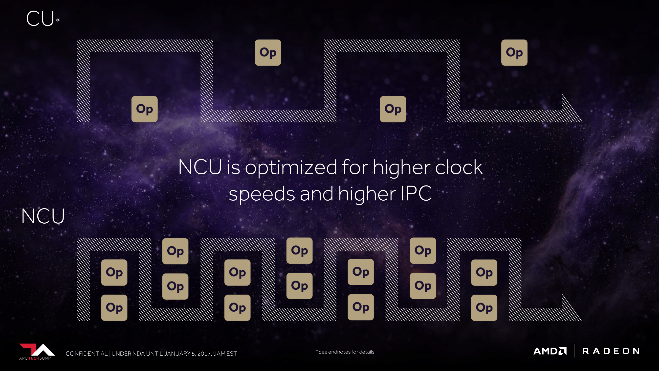
Vega%20Final%20Presentation-29.png
 
Last edited:
Just a heads up none of these products will be available until mid-late 2017, so there is still the possibility of a sort of production exclusivity (or what I think in the case of Nvidia is buying a massive chunk of the production order now-future and so tying it to them), but agree not sure if SK Hynix can be tied down as it has many collaborations although those companies inlcuding AMD probably get preferential orders.

While Altera did go into sampling status Oct 2016 I am not sure it includes the MX family (HBM2 spec version) and the expected shipping date for the MX is mid 2017 earliest.
Looking at Xilinx, the Ultrascale+ HBM (as they call it) is only on a roadmap to date and maybe late 2017, also the product has a spec of 32GB and 64GB HBM2 memory so that cannot be this release.
original


I double checked other sources and seems correct, also re-inforcing this the only Virtex Ultrascale+ eval board available is the DDR4.

I must say I am having problems confirming what memory Xilinx is using (well I guess they were expecting 8Hi so narrows it down, or maybe 8GB density stack fo the 32GB model *shrug*); I am trying to find a specific presentation I have/read that goes into a bit of detail from Xilinx but a nightmare to find.
Cheers


They are listing Gbit not Gbytes -- so 32/64Gb is 4/8GB
 
They are listing Gbit not Gbytes -- so 32/64Gb is 4/8GB
That is a good point and also 1st time I noticed the structure that uses only up to 2 HBM stacks in the largest model, various articles had it as GB rather than Gb bah.
I remember Xilinx going on about 8hi in the past and so did not bother to check the articles as was late, although Xilinx may only had mentioned 8hi from a cooling challenge perspective and viability rather than actual use anytime soon *shrug*.

However it is still only a roadmap like I said, with only the DDR4 eval board available now and expectation that these HBM models will be shipping late in the year (Q3+ and not sure if that is only eval-sampling status).
Xilinx do state though it has a bandwidth of 460GB/s, so quite a performance for a 2-stack and higher than what is currently in the parts catalogue for Sk Hynix or the performance of the Samsung HBM2 inside P100 (depending upon ones view this may/may not be brought down for power purposes).
Could also mean they will use Samsung (still cannot confirm which manufacturer Xilinx are meant to be using) though albeit much later in the year and when production is higher.

Thanks

Edit:
Just noticed mindblank and said TSMC instead of Samsung, now corrected.
 
Last edited:
That isn't entirely true. First of all I remember some site doing some math and making a guess that Fermi was about 20-22 stages of pipeline in each of their cuda cores.

Secondly, AMD was claiming 20% or so higher performance at the same clock with the same shader cound from Fiji/Hawaii -> Polaris.

Lastly, check this slide out, right from AMD: (Sorry It's huge)
Vega%20Final%20Presentation-29.png

That isn't IPC ;)

Edit if they are comparing FP32 to FP16 that picture is correct thought, so yeah in that instance IPC increases are there......
 
Last edited:
That isn't IPC ;)

Edit if they are comparing FP32 to FP16 that picture is correct thought, so yeah in that instance IPC increases are there......
It is still a good point you raise because the slide is deliberatley vague, all one can deduce is higher clock speeds, IPC could be down to as you say the ability of the NCU to mix packed maths.

Cheers
 
I think the main point they are trying to get across is there is occupancy issues in current GCN architectures which the new NCU setup is designed to alleviate -- there for more instructions per clock are computed for the same number of CU's. I DON'T think this is to do with packing math. Just making sure all the execution resources are being used in the first place. Although AMD did claim something like 20% better on Polaris, too.

EDIT: Just checked Polaris whitepaper -- looks like that percentage better on polaris (due to arch and features only, not clock or process) is to do with performance per watt, not performance per cu per clock.
 
I think the main point they are trying to get across is there is occupancy issues in current GCN architectures which the new NCU setup is designed to alleviate -- there for more instructions per clock are computed for the same number of CU's. I DON'T think this is to do with packing math. Just making sure all the execution resources are being used in the first place. Although AMD did claim something like 20% better on Polaris, too.

EDIT: Just checked Polaris whitepaper -- looks like that percentage better on polaris (due to arch and features only, not clock or process) is to do with performance per watt, not performance per cu per clock.
I went back to the Anandtech analysis, they feel the slide is also vague enough to be that the IPC is not clear enough and may be packed maths.
I am not saying it is one or the other just yet, just pointing out it is still very vague and difficult to conclude anything from marketing slides, same could had been said about Polaris from its marketing slides.
Cheers
 
Last edited:
I think the main point they are trying to get across is there is occupancy issues in current GCN architectures which the new NCU setup is designed to alleviate -- there for more instructions per clock are computed for the same number of CU's. I DON'T think this is to do with packing math. Just making sure all the execution resources are being used in the first place. Although AMD did claim something like 20% better on Polaris, too.

EDIT: Just checked Polaris whitepaper -- looks like that percentage better on polaris (due to arch and features only, not clock or process) is to do with performance per watt, not performance per cu per clock.

Hmm.
Looking at the presentation slides that was for the Polaris Tech Day they do look at performance per CU; up to 15% more peformance per CU, 480 compared to 290.
With this footnote:
Testing conducted by AMD performance labs as of May 18, 2016 on the Radeon RX 480 and Radeon R9 290 on a test system comprising Intel Core i7-5960X, 16GB DDR4-2666, Gigabyte X99-
UD4, Windows 10 x64 (build 10586), Radeon Software Crimson Edition 16.5.2using Ashes of Singularity, GTA V, Project Cars, Witcher, and Assassin’s Creed Syndicate, All games tested at 1440p.
Radeon RX 480 graphics (150W TGP/36 CU) vs. Radeon R9 290 graphics (275W TGP/40 CU) scores as follows: Ashes of the Singularity (44.19 FPS vs 46 FPS); GTA V (66.23 FPS vs. 66.44 FPS);
Project Cars (48.99 FPS vs. 45.99 FPS); Witcher 3 (50.78 FPS vs. 50.13 FPS); Assassin’s Creed Syndicate (50.51 FPS vs. 45.78 FPS). Average FPS of above game scores: 52.14 (Radeon RX 480) vs.
50.06 (Radeon R9 290). Discrete AMD Radeon™ GPUs and AMD FirePro™ GPUs based on the Graphics Core Next architecture consist of multiple discrete execution engines known as a
Compute Unit (“CU”). Each CU contains 64 shaders (“Stream Processors”) working in unison (GD-78). CU efficiency formula = average FPS/# of CUs. Test results are not average and may vary.
RX-4
http://radeon.com/wp-content/uploads/2016/08/Polaris-Tech-Day-Architecture-Final-6.24.2016.pdf

Anyway due to Vega having various efficiency-performance acceleration functions as well that seem to be bundled in some general figures, I think we need more details about the IPC with NCU until we can conclude much about the Vega slide apart from higher clocks supported by the NCU.

Thanks
 
Last edited:
Separate to the above, did AMD ever go into the IPC of Polaris or even Fiji when compared to Hawaii/Tonga?
Serious question as not sure how it really fits this time with what we have been told so far.
Thanks
 
I'm just gonna say this: As a dev, an API is only as good as its usability. An API should conform to the devs' wants and needs, not the other way around. It's not AMD's fault that devs want something that differs from the OpenGL spec, but when you look at the landscape and how many devs differ from the spec, maybe AMD should've joined Nvidia and asked the Khronos group to change the spec to reflect what the devs are actually using and running.

Versioning is there for a reason, AMD just allowed themselves to fall behind by being too rigid. Now that Nvidia has the huge marketshare, Nvidia's spec might as well be the official spec, since they represent most of the market and most of the customers.
You are only referencing PC and foregoing the greater share when considering consoles. Like it or not Consoles still have a huge impact on API and the groundwork for most games ( ie: game is made for console first ).
 
OK found the footnote for the CU vs NCU slide that mentions higher clocks and IPC:
CU vs Vega NCU slide: Discrete AMD Radeon and FirePro GPUs based on the Graphics Core Next architecture consists of multiple discrete execution engines known as a Compute Engine ("CU").
Each CU contains 64 shaders ("Stream Processors") working together.

Just to add I agree it is possibly about balancing/occupancy than an actual hard figure that can be calculated like TFLOPs, but unfortunately still cannot rule out fully packed maths as being inferred by the slide for IPC.
Cheers
 
Last edited:
You are only referencing PC and foregoing the greater share when considering consoles. Like it or not Consoles still have a huge impact on API and the groundwork for most games ( ie: game is made for console first ).

AFAIK OpenGL is used in none of the consoles, so I'm not sure how that's relevant?
 
I went back to the Anandtech analysis, they feel the slide is also vague enough to be that the IPC is not clear enough and may be packed maths.
I am not saying it is one or the other just yet, just pointing out it is still very vague and difficult to conclude anything from marketing slides, same could had been said about Polaris from its marketing slides.
Cheers
:ROFLMAO:, another AMD slide that can be thrown in the toilet because it really doesn't show anything meaningful. Man I am beginning to hate how AMD presents information that is no information at all. :mad:

Better off just ignoring that stuff and wait for real tests to come out.
 
AFAIK OpenGL is used in none of the consoles, so I'm not sure how that's relevant?
speaking more to now not opengl. Called a parallel. I akin it a lot to ENB. The inventor is world renowned for his work, as well he should be, but he is an absolute ASS and an avid Nvidia fanboy. Therefore those of us with AMD hardware have to put up with the inefficiencies if we want what it brings ( I don't, I just use the memory patch ). This is akin to a lot of software out there right now, inc VR. They favor Nvidia because that is unfortunately what those writing it use. And sometimes, or even most, the writer is an ass and codes only for Nvidia, AMD be damned.
 
speaking more to now not opengl. Called a parallel. I akin it a lot to ENB. The inventor is world renowned for his work, as well he should be, but he is an absolute ASS and an avid Nvidia fanboy. Therefore those of us with AMD hardware have to put up with the inefficiencies if we want what it brings ( I don't, I just use the memory patch ). This is akin to a lot of software out there right now, inc VR. They favor Nvidia because that is unfortunately what those writing it use. And sometimes, or even most, the writer is an ass and codes only for Nvidia, AMD be damned.

I see, everyone but AMDs fault again.
 
speaking more to now not opengl. Called a parallel. I akin it a lot to ENB. The inventor is world renowned for his work, as well he should be, but he is an absolute ASS and an avid Nvidia fanboy. Therefore those of us with AMD hardware have to put up with the inefficiencies if we want what it brings ( I don't, I just use the memory patch ). This is akin to a lot of software out there right now, inc VR. They favor Nvidia because that is unfortunately what those writing it use. And sometimes, or even most, the writer is an ass and codes only for Nvidia, AMD be damned.

How's that relevant to my OpenGL vs Vulkan point? I don't see the parallel, someone help me understand. :confused:
 
speaking more to now not opengl. Called a parallel. I akin it a lot to ENB. The inventor is world renowned for his work, as well he should be, but he is an absolute ASS and an avid Nvidia fanboy. Therefore those of us with AMD hardware have to put up with the inefficiencies if we want what it brings ( I don't, I just use the memory patch ). This is akin to a lot of software out there right now, inc VR. They favor Nvidia because that is unfortunately what those writing it use. And sometimes, or even most, the writer is an ass and codes only for Nvidia, AMD be damned.
OpenGL has been under control of Khronos Group since 2006, that is plenty of time and iterations for it to be under control of a broad committee beyond what you feel is the influence of Nvidia.
Do you complain about OpenCL that was created by Apple and is also under Khronos Group?
Cheers
 
speaking more to now not opengl. Called a parallel. I akin it a lot to ENB. The inventor is world renowned for his work, as well he should be, but he is an absolute ASS and an avid Nvidia fanboy. Therefore those of us with AMD hardware have to put up with the inefficiencies if we want what it brings ( I don't, I just use the memory patch ). This is akin to a lot of software out there right now, inc VR. They favor Nvidia because that is unfortunately what those writing it use. And sometimes, or even most, the writer is an ass and codes only for Nvidia, AMD be damned.

I don't know if you were around at the time but back in the early days of 3d acceleration NV worked HARD on their OpenGL drivers so that they could start securing "wins" over GLide in the Quake engine (It was Quake2 where they made massive strides IIRC). NV was throwing out new drivers left and right and was able to go from no OpenGL support at all to parity with GLide purely through the drivers. It was pretty damn epic to experience if you had a Riva TNT at the time (maybe 128? It seems like centuries ago). This is where NV forged their "NVIDIA has the best drivers" label among the PC community and went from the underdog to on top which was cemented with the release of the first GeForce, stable OpenGL drivers, and a new game called Quake 3 Arena.

At least that's how I remember it; awesome times for sure.
 
http://wccftech.com/amd-radeon-rx-500-vega-10-vega-11-gpus/

Take with the usual source criticism. But Vega 11 may only have 1 4GB HBM2 stack at 205-256GB/sec.

Gotta call shens on that one. With the vram usage of most all AAA games now, not including the "high res textures" packs, I don't see anyone releasing anything remotely enthusiast level with less than 8GB anymore. Now Vega 11 is supposed to be mid-range replacement for Polaris 10, but I still don't see them using less than 6GB. When Vega 10 is supposed to be 8-16GB, and Vega 20 is supposed to be up to 32GB. But stranger shit has happened heh
 
Gotta call shens on that one. With the vram usage of most all AAA games now, not including the "high res textures" packs, I don't see anyone releasing anything remotely enthusiast level with less than 8GB anymore. Now Vega 11 is supposed to be mid-range replacement for Polaris 10, but I still don't see them using less than 6GB. When Vega 10 is supposed to be 8-16GB, and Vega 20 is supposed to be up to 32GB. But stranger shit has happened heh

People didn't believe 4GB Fiji either.

8hi stacks is the nemesis again.
 
Gotta call shens on that one. With the vram usage of most all AAA games now, not including the "high res textures" packs, I don't see anyone releasing anything remotely enthusiast level with less than 8GB anymore. Now Vega 11 is supposed to be mid-range replacement for Polaris 10, but I still don't see them using less than 6GB. When Vega 10 is supposed to be 8-16GB, and Vega 20 is supposed to be up to 32GB. But stranger shit has happened heh


Its not a limitation on what they can or cannot do, if they plan on using HBM 2 on this chip, it could be the price of HBM 2 with more stacks will not allow them to be in a mainstream price range.
 
I think AMD betted on the following long ago when these parts was planned:

No such thing as GDDR5X/GDDR6.
8Hi HBM2 stacks to exist and be common.
2Ghz HBM2 as a standard, possible faster speeds.
Lower cost for HBM2 parts and higher volume to drive down price.
 
So how effective will the Cache controller be? Fiji runs with 4gb where other 4gb cards would have an issue and it does not have a cache controller. I think I would rather have the 8gb + cards but am interested if their is a clear benefit with the new Tech. Also will HBM2 be combined with other ram on the lower end? Could get interesting but bottom line is how it performs and at what cost.
 
So how effective will the Cache controller be? Fiji runs with 4gb where other 4gb cards would have an issue and it does not have a cache controller. I think I would rather have the 8gb + cards but am interested if their is a clear benefit with the new Tech. Also will HBM2 be combined with other ram on the lower end? Could get interesting but bottom line is how it performs and at what cost.


Cache Control is a memory controller lol, no real differences for gaming, Scott Wasson stated this in one of his interviews, it will make a difference for SGG products, but that is about it, transferring over the pci-e bus will always be a bottleneck for the near future. But since the hard drive is on the card PCB no longer have to worry about the pci-e bus being a bottleneck.

Now for systems that have tech like n-link, can't think of AMD's term for their tech right now but that tech will go into servers, it will come in handy as well. Gotta remember nV also has something similar in their HPC and server tech that use nv-link too.
 
Gotta call shens on that one. With the vram usage of most all AAA games now, not including the "high res textures" packs, I don't see anyone releasing anything remotely enthusiast level with less than 8GB anymore. Now Vega 11 is supposed to be mid-range replacement for Polaris 10, but I still don't see them using less than 6GB. When Vega 10 is supposed to be 8-16GB, and Vega 20 is supposed to be up to 32GB. But stranger shit has happened heh
That depends on how you measure memory. No reason the cards couldn't have a secondary pool like SSG. Vega 11 in theory releases with Snowy Owl APUs at which point it could be valid to add in the entire system memory capacity/bandwidth to the card for textures.

Even for Vega11 I see no reason it couldn't be a 32GB or larger part beyond practicality. Should be ample space to stack HBM on an interposer with a smaller die. Having different 4-8GB models for price points and/or salvage wouldn't be unreasonable.

Cache Control is a memory controller lol, no real differences for gaming, Scott Wasson stated this in one of his interviews, it will make a difference for SGG products, but that is about it, transferring over the pci-e bus will always be a bottleneck for the near future. But since the hard drive is on the card PCB no longer have to worry about the pci-e bus being a bottleneck.

Now for systems that have tech like n-link, can't think of AMD's term for their tech right now but that tech will go into servers, it will come in handy as well. Gotta remember nV also has something similar in their HPC and server tech that use nv-link too.
HBCC looks more like a memory manager than a memory controller. A controller capable of tracking a large number of buffers and managing them far more efficiently than would be possible with software. Games do demonstrate a performance difference in how well memory is managed and AMD listed ~50% memory as not being actively used in current games (may have been a worst case scenario, they didn't specify). Vega10 was mentioned to have 32x PCIE3 lanes by an engineer. A 32x PCIE slot is theoretically possible with the standard, albeit a bit long. In the case of the APUs (Snowy Owl/Vega11? and Naples/Vega10/11) there's no reason that traditional PCIE limit will still exist. An integrated part would use Infinity/xGMI and be more configurable. A dual package product theoretically would be 8x (16x slot / 2) to each chip then 24x lanes between without a bridge for a shared pool. A discrete card potentially with 16x lanes idle or to a secondary pool on the board. A few more memory chips for a premium part wouldn't be unreasonable or overly expensive. $50-100 more and adding 16-32GB DDR in addition to HBM2 wouldn't be unreasonable.

I'm still of the mindset the APUs will be the more disruptive part as that interconnect is far easier to achieve without the added costs of a secondary memory pool.
 
That depends on how you measure memory. No reason the cards couldn't have a secondary pool like SSG. Vega 11 in theory releases with Snowy Owl APUs at which point it could be valid to add in the entire system memory capacity/bandwidth to the card for textures.

Even for Vega11 I see no reason it couldn't be a 32GB or larger part beyond practicality. Should be ample space to stack HBM on an interposer with a smaller die. Having different 4-8GB models for price points and/or salvage wouldn't be unreasonable.


HBCC looks more like a memory manager than a memory controller. A controller capable of tracking a large number of buffers and managing them far more efficiently than would be possible with software. Games do demonstrate a performance difference in how well memory is managed and AMD listed ~50% memory as not being actively used in current games (may have been a worst case scenario, they didn't specify). Vega10 was mentioned to have 32x PCIE3 lanes by an engineer. A 32x PCIE slot is theoretically possible with the standard, albeit a bit long. In the case of the APUs (Snowy Owl/Vega11? and Naples/Vega10/11) there's no reason that traditional PCIE limit will still exist. An integrated part would use Infinity/xGMI and be more configurable. A dual package product theoretically would be 8x (16x slot / 2) to each chip then 24x lanes between without a bridge for a shared pool. A discrete card potentially with 16x lanes idle or to a secondary pool on the board. A few more memory chips for a premium part wouldn't be unreasonable or overly expensive. $50-100 more and adding 16-32GB DDR in addition to HBM2 wouldn't be unreasonable.

I'm still of the mindset the APUs will be the more disruptive part as that interconnect is far easier to achieve without the added costs of a secondary memory pool.

APU's are still bound by the same metrics, your direct memory pool or cache pool will still be ram instead of vram, then your bottleneck will shift over to the other component connectors, which have less bandwidth than the ram to the APU.
 
APU's are still bound by the same metrics, your direct memory pool or cache pool will still be ram instead of vram, then your bottleneck will shift over to the other component connectors, which have less bandwidth than the ram to the APU.
All the graphics that have leaked out always had a CPU to GPU interconnect on the APUs that was sufficient to accommodate all system memory bandwidth. There shouldn't be any other component connectors involved. The GPU/APU has it's own limited high performance VRAM pool then some form of secondary storage for textures which won't require all the bandwidth of ROPs in a reasonably efficient system. As I mentioned in that post, a dual Vega10 in theory can accommodate 24x lanes just to send data back and forth with reasonably low latency. An APU with Infinity between CPU and GPU I'd expect to be able to scale that bandwidth to whatever is required with even better performance than PCIE. So even a mid range APU would have 4/8GB(?) HBM2 in addition to whatever system memory could provide that isn't constrained by a connector. A Vega10 APU would have 32x PCIE3 lanes connecting it to the CPU, that should be more than sufficient for overflow at 32GB/s. The xGMI or other link should outperform that as the connection is extremely short existing over an interposer.
 
All the graphics that have leaked out always had a CPU to GPU interconnect on the APUs that was sufficient to accommodate all system memory bandwidth. There shouldn't be any other component connectors involved. The GPU/APU has it's own limited high performance VRAM pool then some form of secondary storage for textures which won't require all the bandwidth of ROPs in a reasonably efficient system. As I mentioned in that post, a dual Vega10 in theory can accommodate 24x lanes just to send data back and forth with reasonably low latency. An APU with Infinity between CPU and GPU I'd expect to be able to scale that bandwidth to whatever is required with even better performance than PCIE. So even a mid range APU would have 4/8GB(?) HBM2 in addition to whatever system memory could provide that isn't constrained by a connector. A Vega10 APU would have 32x PCIE3 lanes connecting it to the CPU, that should be more than sufficient for overflow at 32GB/s. The xGMI or other link should outperform that as the connection is extremely short existing over an interposer.


So you don't think having HBM on an interposer is an advantage either? This is also about latency too. Bandwidth and latency are important in those factors, you can't tell me a HD connected through a sata connector has the same bandwidth and latency as accessing ram.
 
Scorpio might be an APU with HBM stacks. The fixed memory size is expected for that use case.

But here's one - Pure speculation and not about anything currently announced necessarily.

What if they go to an all APU product stack? Think SMP but with one of the 'sockets' attached via PCIe. There was a lot of talk about enhancements to Hypertransport a few years ago and the SeaMicro acquisition that didn't seem to go anywhere.
(ref http://www.theinquirer.net/inquirer/news/2162252/amd-bought-seamicro-interconnect-fabric and https://arstechnica.com/uncategorized/2006/06/6977-2/)

Now they are talking up memory coherency for discrete GPUs which isn't so far off from the Hypertransport based co-processor concept they talked about

Current APUs are about 60% CPU and 40% GPU. APUs and traditional CPUs connect to the rest of the system primarily via PCIe.

Now imagine a system with an typical APU/CPU connected via PCIe to a coprocessor APU that's 80-90% GPU and uses the rest of the die for, say 2 CPU cores. Clever driver or API techniques could push the graphics related threads to that 'socket' minimizing critical path latency for rendering. AMD's NUMA has allowed asymmetric memory pools for years so that's not an issue.

This would open up interesting low power modes where only the processor driving the display needs to be active. Dockable/modular processing like the Alienware graphics amplifier would also get a lot more interesting.
 
Until seen, the options are there for AMD or AIBs to do some interesting stuff with their new Memory/Cache/controller/manager however you want to look at it. 4GB HBM2 maybe not too much of a limitation on the mainstream cards but we will not know if AMD will be successful in such a configuration, unless for one they release another 4GB HBM card with the memory cache controller. If additional resources will be on the card such as GDDR3/5 SSD will have to be seen.

I thought the HardOCP review with Fallout 4 High Res Texture DLC was very interesting in that yes the Fury X was able to handle a memory pool way above 4gb and run the game but in the end it stuttered. Will an updated driver make this better? (It was tested on a rather high end system). I will test with my Nano with a PCIe SSD to see if that stutter is still present. In short yes Fiji is able to handle it but I would call it a fail as well due to the stutter of HardOCP tests. I would not predict either way that a 4GB HBM2 card will be able to handle the same test better or worst. In this case I hope HardOCP keeps Fallout 4 with High Res Texture Pack in their gaming test suite.
 
So you don't think having HBM on an interposer is an advantage either? This is also about latency too. Bandwidth and latency are important in those factors, you can't tell me a HD connected through a sata connector has the same bandwidth and latency as accessing ram.
There's no requirement that the SSG tech uses a hard drive of any type. It's simply block IO on whichever controller they choose to connect via PCIE. There's a 128Gb/s fibre channel spec that lines up rather nicely with 16x PCIE3. That seems likely for the datacenter. They could build a custom NVMe setup or make a ramdrive. DDR3 for a cheap secondary pool would be reasonably low latency and respectable bandwidth if they went that route.

What if they go to an all APU product stack? Think SMP but with one of the 'sockets' attached via PCIe. There was a lot of talk about enhancements to Hypertransport a few years ago and the SeaMicro acquisition that didn't seem to go anywhere.
Far easier to just make a bigger APU to start with unless they want variably configured consoles. Consoles likely have the chips mounted to the board without a socket as well. I wouldn't be surprised if we see future APU systems where the APU is fixed to a SFF motherboard with a chassis designed around it.

I thought the HardOCP review with Fallout 4 High Res Texture DLC was very interesting in that yes the Fury X was able to handle a memory pool way above 4gb and run the game but in the end it stuttered.
Keep in mind AMD created the SSG because going through the CPU to access storage of even system memory was still problematic. They had demos showing the benefits of a dedicated drive. I'd expect those benefits to help that stuttering situation with lower latency, never mind the obviously increased bandwidth.
 
Keep in mind AMD created the SSG because going through the CPU to access storage of even system memory was still problematic. They had demos showing the benefits of a dedicated drive. I'd expect those benefits to help that stuttering situation with lower latency, never mind the obviously increased bandwidth.
Although that was comparing to SSD storage and loading and not system RAM, developers could do much more with system RAM with regards to creating a more dynamic unified memory pool espcially where people have 16GB or 32GB but there is no incentive in same way for the developers to use VRAM efficiently.
For SSG to benefit games though the developer still needs to interact with it and Raja touched upon this very briefly in an interview, without that intervention its benefits are a bit more limited.
Cheers
 
There's no requirement that the SSG tech uses a hard drive of any type. It's simply block IO on whichever controller they choose to connect via PCIE. There's a 128Gb/s fibre channel spec that lines up rather nicely with 16x PCIE3. That seems likely for the datacenter. They could build a custom NVMe setup or make a ramdrive. DDR3 for a cheap secondary pool would be reasonably low latency and respectable bandwidth if they went that route.

Data Centers, Server, HPC, AMD is in competition with nV, nV already same similar tech in that regard for those markets.

Keep in mind AMD created the SSG because going through the CPU to access storage of even system memory was still problematic. They had demos showing the benefits of a dedicated drive. I'd expect those benefits to help that stuttering situation with lower latency, never mind the obviously increased bandwidth.

And would an SSG be cost beneficial to the game market? Above you stated they seem to be more for data centers..... and also Scott Wasson already stated without the SGG the benefits are limited in current platforms. Actually his words were more like there is no benefit currently in gaming.
 
Far easier to just make a bigger APU to start with unless they want variably configured consoles. Consoles likely have the chips mounted to the board without a socket as well. I wouldn't be surprised if we see future APU systems where the APU is fixed to a SFF motherboard with a chassis designed around it.
I was thinking CPU cores in their GPUs. Effectively an APU but the other way around
 
Back
Top