N4CR
Supreme [H]ardness
- Joined
- Oct 17, 2011
- Messages
- 4,947
Ram speed is where it gets interesting with the differences of HBM design. This is why everyones unsure about it. No doubt if they are/have done it, will be some logical wayI am very interested in the infinity fabric. I would assume it will use pci-e x16 like the cpu, however what will be the speed? Will it be tied to ram speed? Not sure how much correlates with the CPU.
But that also leads to Simplyfuns' post which is probably bang on the money.
This sounds about right. E.g. 50% scaling only, or some sort of frame time/pacing issue.I think AMD is about to make mGPU a "thing" that is invisible to whatever is making the calls. Given their past history, I think it will work, but ver 1 will have quirks we don't like.
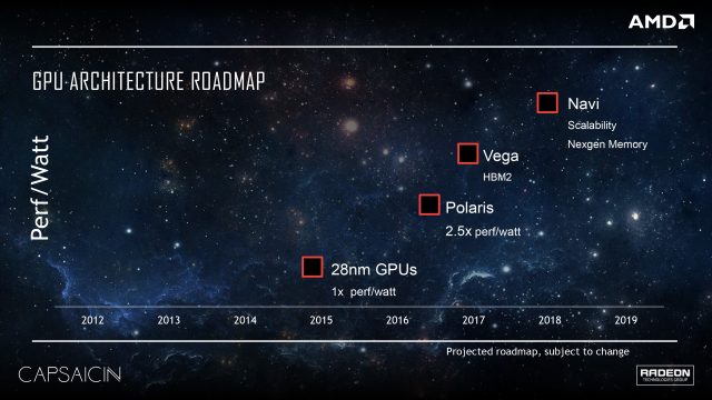
This is RTGs only real ticket to high end competition for next few years though and could be similarly disruptive as Naples could potentially be.
E.g. we may see as following
Vega 10: OCd 1080 to Ti or faster in some games.
Gv104 ~Ti speed range
Nvidia is still tied with AMD for overall performance until they get Gv102 out later. Of course the power use shilling will be in overdrive during this time.
Gv102 launches 2018, usual +50-60% with a much bigger die than Gp102, clock bump, some process refinements as usual, Titan, ten gorillion dollars.
AMD counters with Vega10x2, matches or takes crown back (I doubt it will be ready this year but please prove me wrong AMD) costs a little less.
>PowerUseShillingIntensifies.webm
late 2018 dec Nvidia releases Volta Ti 'Titan watered down edition because we can't sell any more for HPC first'
AMD releases Navi, drawing nearly even on process this time (7nm gloflo)
Nvidia releases Ti 'watered down edition Titan with a cost cut and less ram' and some 'even less watered down edition' Titan with more ram than the last one and a clock bump
MCM process repeats (note how they expect Vega10x2 much sooner than the usual year between single and dual GPU launches...) as they now make MCM/mGPU cards part of key R&D
High end is now muddied. AMD offers higher performance and slightly higher power usage.
Epeen upgraditis types now confused 'cus muh Nvidia is not so stronk all of a sudden and 'AMD SUXX LOLOLOL' can't be so easily played when they're competitive or better on performance.
Next few years are going to be a great time for GPU consumers... 4k, 8k, VR, mGPU/MCM bring it on!
")