![[H]ard|Forum](/styles/hardforum/xenforo/logo_dark.png)

- Joined
- Dec 19, 2005
- Messages
- 18,427

"As a first step towards real implementations, imec demonstrated memory operation of the CCD with IGZO on a 2D proof-of-concept. The planar CCD structure of this 2D proof-of-concept consists of an input stage, 142 stages (each consisting of four phase gates) which can each store one bit, and a two-transistor-based read-out stage. The CCD register is written by injecting charges through the input stage and sequentially transferring them through all 142 stages by switching the voltages of the phase gates. The CCD offers more than 200s retention, an endurance of >1010 cycles without degradation, and a charge transfer speed exceeding 6 MHz. Multilevel storage capability of the CCD register was also demonstrated, contributing to a higher bit density. Being widely adopted in the image sensor market, the charge-based CCD technology is well-known, reliable, and can operate at low voltages - benefiting power consumption."
Maarten Rosmeulen, Program Director Storage Memory at imec: "The real value of the proposed buffer memory lies in its ability to be integrated into 3D NAND fashion, with IGZO-based CCD registers integrated into vertically aligned plugs - a concept that we now propose for the first time. From what is possible with NAND Flash today (i.e., the capability of processing 230 layers), we estimate that our 3D buffer memory can already provide five times more bit density than what (2D) DRAM is expected to offer in 2030. We are currently investigating real 3D implementations with limited number of word lines."
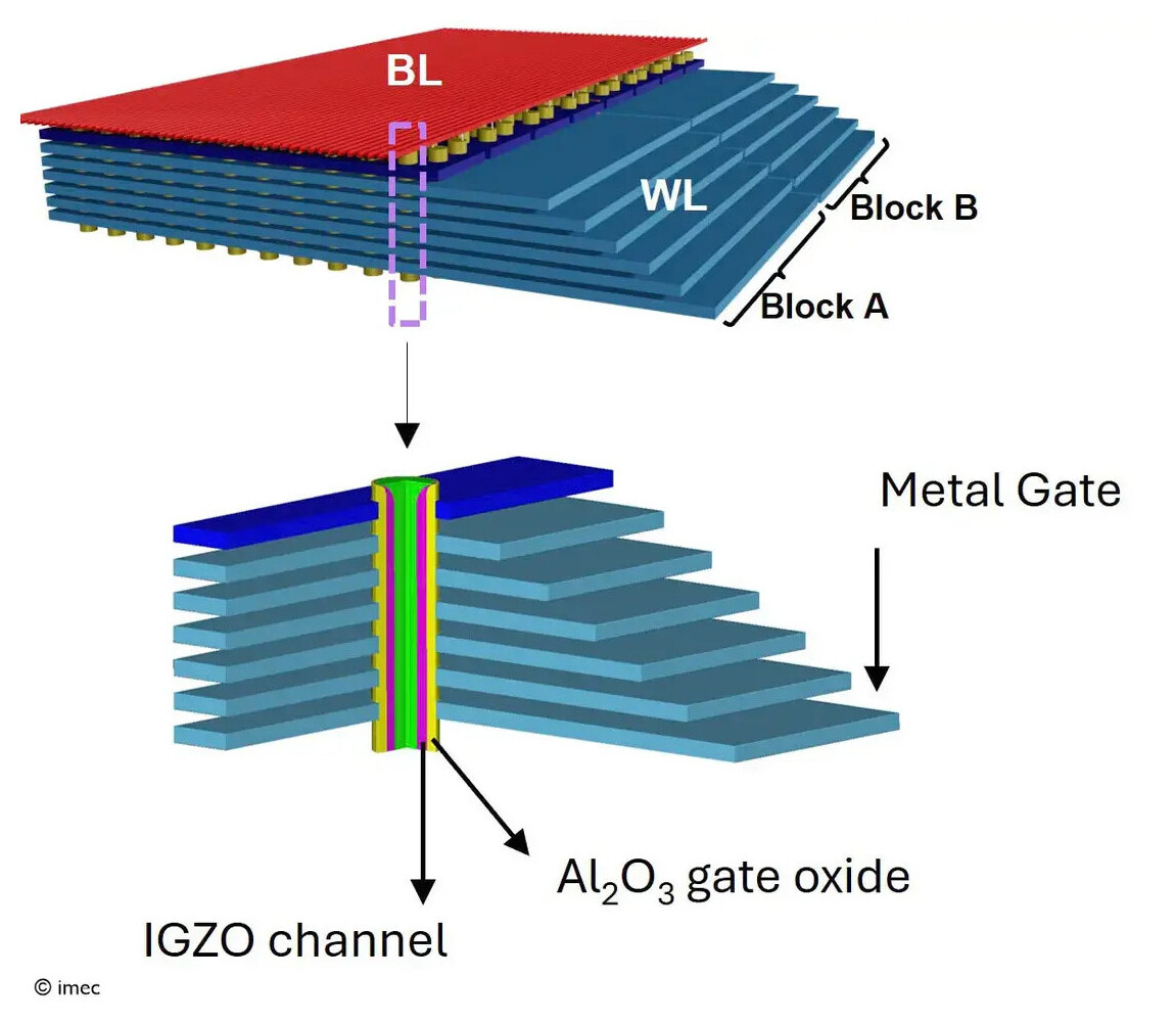
Source: https://www.techpowerup.com/329779/...er-memory-that-could-surpass-dram-bit-density