Shintai
Supreme [H]ardness
- Joined
- Jul 1, 2016
- Messages
- 5,677
R&D Budget: $3B USD
https://devblogs.nvidia.com/parallelforall/inside-volta/
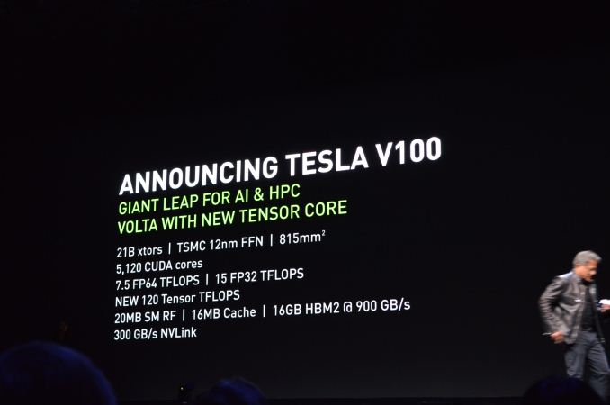
Volta 50% more power efficient than Pascal.
1455Mhz, down from 1480Mhz with GP100.
Samsung 1.75Ghz HBM2.
320 TMUs (+50% vs GP100)
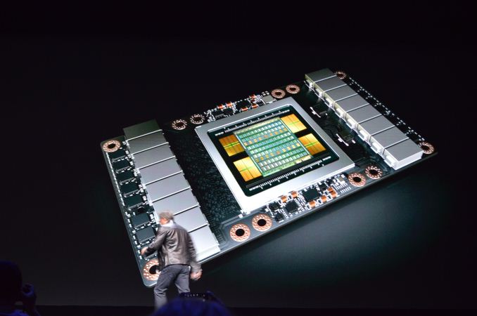
TSMC 12nm FFN, a 4th generation 16nm made specially for Nvidia with their demands.
Maxed out the reticle size of TSMC’s process.
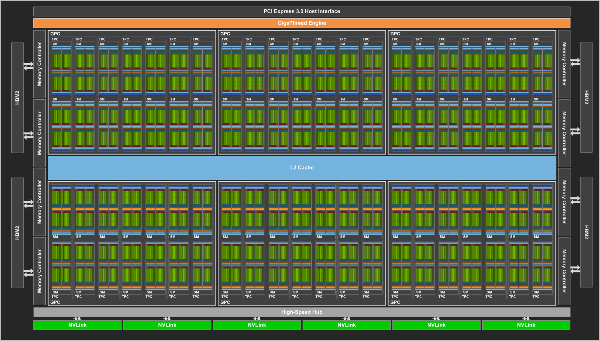
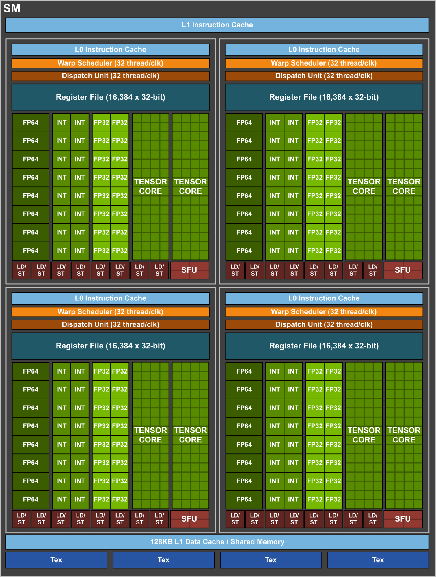
5376 Cuda cores on the chip, 4 SMs disabled for yield like GP100.
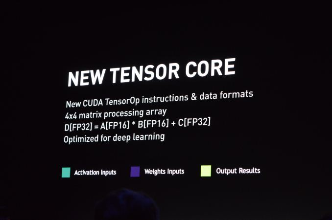
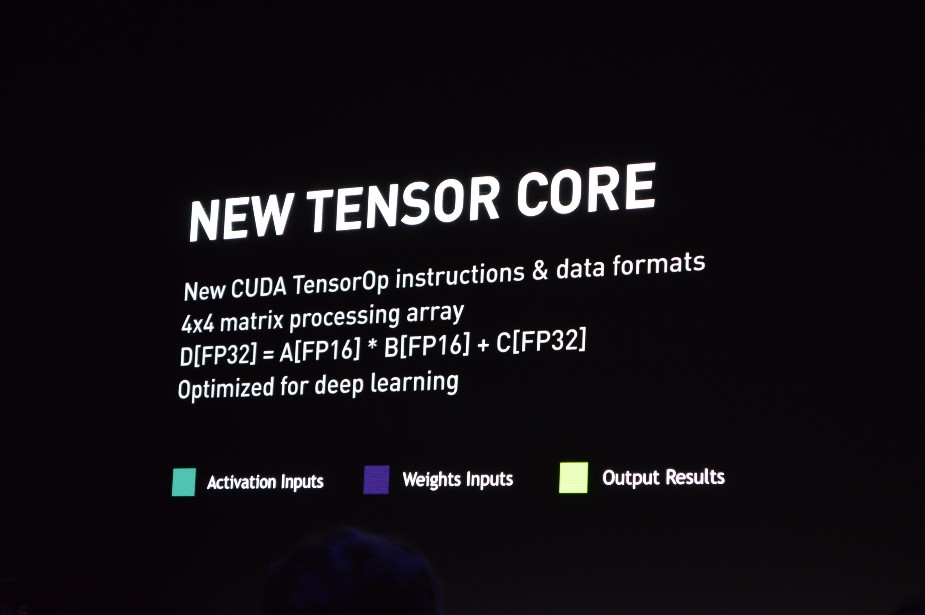
30Tflops FP16, 120Tflops Tensor.
300W card.
NVlink 2.0.
Full height, half length 1 slot 150W lower clocked card as well.
FP32 and INT32 are now separate cores (can operate independently and in parallel).

https://devblogs.nvidia.com/parallelforall/inside-volta/
Volta 50% more power efficient than Pascal.
1455Mhz, down from 1480Mhz with GP100.
Samsung 1.75Ghz HBM2.
320 TMUs (+50% vs GP100)
TSMC 12nm FFN, a 4th generation 16nm made specially for Nvidia with their demands.
Maxed out the reticle size of TSMC’s process.
5376 Cuda cores on the chip, 4 SMs disabled for yield like GP100.
30Tflops FP16, 120Tflops Tensor.
300W card.
NVlink 2.0.
Full height, half length 1 slot 150W lower clocked card as well.
FP32 and INT32 are now separate cores (can operate independently and in parallel).


Last edited: