What ever happend to the 800MHz FSB?

Kato1144

Limp Gawd
Joined
Oct 18, 2007
Messages
354
I was watching an XP build on youtube by AkBKuKu on his TechTangents channle and he is using an old P4 550, now I forgot untill I was watching this video but back then intel was running there FSB at 800MHz... now i think AMD was also doing this with there AMD64 platform, i do recall seening a FSB for an AMD cpu at the time being like 400MHz, now i know these speeds were the system bus speed of around 100MHz hit with a muiliplyer as it came to the CPU for the mad bus speeds and at the time it looked like that was the direction of CPU's, intel and AMD were hitting higher and higher FSB speeds and soon the 10GHz CPU that intel was talkinga about was going to be the future. Anyway I personally fell off of the PC train around 2005 to about 2009 and when i got back it was all Core2duo and Phenom CPU's that had taken over the market and the days of insain FSB speeds was over so now being reminded of the past I'm curious on what happend to the philosophy of faster and faster FSB speeds, like if you asked me to predict the future of CPU's back in 2005 I would have thought that the FSB speeds would have kept increasing along with CPU speeds.


Now I do have a theory as to why, the 800MHz FSB speed that intle was using was generated on the MOBD probly by the north bridge and so making a faster FSB you needed to be depended on the MOBD chip set, so I'm gussing that when the memory controller and most of the NB chipset got integrated in to the CPU so did the crazy FSB speeds that the CPU needed, keeping the system Bus speed at 100MHz, really now it's just the memory speed that is faster then the Bus speed now as far as I can tell and that talks directly to the CPU so ya I gusse no more need for 800MHz FSB.

Anyway this was a fun little think on the past that I grew up with, durring one of the more interesting times in computer hardware history and figured I would ask what happend to the insain FSB of yesteryear.
 
You still have a FSB clock speed but it is just more advanced than that.

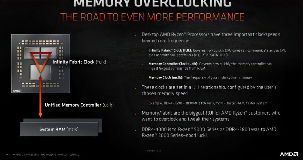
On an Amd CPU it is still around it is just called fclk and uclk. It is the bus that communicates between the System Memory, Memory Controller, and the CCX's, The fclk is the bus that communicates between the CPU and the other SOC components on the die.

So basically you can just think of it as an evolution of the traditional FSB. The funny thing about the fclk and uclk is that it communicates way faster than the 800mhz FSB of yesteryear.

1667225914259.png
 
Last edited:
Current CPU's use PCI-E to communicate between CPU and PCI-E devices hence your bus really is mostly PCI-E and because of that it is 100MHz since 100MHz is reference clock for PCI-E
Chipsets (and thus CPU's!) are said to use different buses but they are pretty much just PCI-E devices acting as PCI-E hubs with integrated devices (USB, SATA, etc. ports and some other functionalities).
Bus can also be used to communicate between two or more CPU's and it is these multi-processor systems where all the differences between raw PCI-E and current buses lie (Intel QuickPath Interconnect and AMD Infinity Fabric)

BTW. FSB bus on Core 2 was the same FSB bus that was used for all Netburst processors (Pentium 4 and Pentium D) and it had really 1/4 clock of stated clock so your 800MHz was really 200MHz. Beefiest Core 2 processor C2D QX9770 and QX9775 used 1600MHz bus so really 400MHz. I personally used >500MHz bus on my Core 2 Duo E7200 😎
The high MHz numbers are just pure marketing. The same marketing could be used for PCI-E to increase its perceived clock rates and actually match real clocks used for PCI-E bus

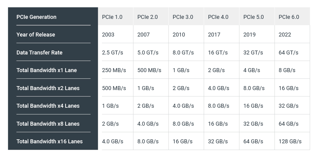
PCIe GenerationsBandwidthGigatransferFrequency
PCIe 1.08GB/s2.5GT/s2.5GHz
PCIe 2.016GB/s5GT/s5GHz
PCIe 3.032GB/s8GT/s8GHz
PCIe 4.064GB/s16GT/s16GHz
PCIe 5.0128GB/s32GT/s32GHz

I would assume that since something like Intel Raptor Lake has 16 lanes of PCI-E 5.0 it also runs Intel QuickPath Interconnect at 32GHz for communicating with Z790 chipset and 16GHz for Z690 chipset.

tl;dr
Current CPUs have 32000MHz bus speeds
32000MHz >>> 800MHz 🥳

ps. FSB ran at 64 bits == lanes so difference between maximum data rates in/out CPU is less than difference in clocks.
To calculate this one would have to add up all QPI and PCI-E lanes at their rated maximum supported modes and divide by 64-bit FSB at 800MHz
 
Last edited:
Ya that makes sense, as the CPU became more integrated the Bus for the memory controller and such were moved in to the CPU its self and now the FSB is just the PCIe refrence speed, the reminds me at the start of the i7 era ppl who were overclocking were told to advoid clocking the FSB to much because it was now linked to the PCIe clock speed and could mess up you PCIe devices and now in this day and age overclocking is primary done with the multiplier.

now for the PCIe 5.0 bus speed I'm alittle confused on what is going on there 32GHz seems like alot but then again PCIe is borken up in to lanes and I did a little math and looked at a PCIe reference sheet.
PCIe-Blog-Chart-EN.jpg


so for a 5.0 PCIe connector we have a Data transfer rate of 32 GT/s witch you say is about 32GHz of speed, now is that like 32GHz per lane or is it the top combined speed of each lane added togeather 2GHx16=32GHz?


with that said if it is 32GHz per lane at all times that pretty wild and i had no idea that we were in the multi GHz ranged with inter CPU communication to devices, I know that multi GHz frequencys are not to far fetched and it comes down to the CPU architecture, the process of the node and so on but I gusse i did not think the CPU would be hitting the PCIe lanes with 32GHz of frequency just seems like alot and one hell of a multiplier using the 100MHz refrence clock, thats a multiplier of x320 so if you over clock your 100Mhz FSB like by 10MHz you would get a real clock on the PCIe bus of like 35.2GHz that 3.2GHz more form a 10MHz bump.

ps. FSB ran at 64 bits == lanes so difference between maximum data rates in/out CPU is less than difference in clocks.
To calculate this one would have to add up all QPI and PCI-E lanes at their rated maximum supported modes and divide by 64-bit FSB at 800MHz
Also not to sure what you mean here my dude, its most likly im missing some fundamentals that i would need to undersatnd waht your putting down here.

My understanding level of what bits mean :p
 
For serial data transmission it is best to go to basics.
Say we have COM port at baud rate 9600. It means you can transmit or receive 9600 bits per second in either direction. This translates to 1200 bytes/second or 150 64-bit words/second.
If you wanted to have bidirectional connection (be able to send and receive independently) then you could setup two COM connections at the same time, one for receiving and one for transmitting.
If you wanted to increase bandwidth you could either increase baud rate - same thing as transfers per second !!! - or increase number for COM connections eg. 8 COM (or COM pairs) you could transmit 9600 bytes per second.

PCI-E 5.0 1x is like COM port pair (one always transmitting and one receiving, just with stupendous 32'000'000 baud rate.

FSB but (otherwise for Core2 called AGTL+ bus) is 64-bit and is bi-directional. In simple terms is like having 64 lanes of PCI-E operating at 800MHz or 64 pairs of COM ports (or 128 in total) operating at 800'000 baud rate.

FSB @ 800MHz compared to PCI-E 5.0 1x has 40x lower frequency but 64x times lanes so its 1.6x faster for transferring data, 6.4GB/s of FSB vs 4GB/s of PCI-E 5.0 1x.
In the past FSB was used not only to communicate with devices but also to communicate with memory so it had to be pretty fast. Preferably as fast as memory itself to avoid bottlenecks. If FSB was slower than memory then CPU could not utilize maximum bandwidth offered by memory and this was not desirable. Memory at Core2 times operated at 400MHz (really 200MHz DDR) and 128-bit (in dual-channel, each stick of RAM being 64-bit) so 800MHz bus at 64-bit was perfectly adequate.

Also not to sure what you mean here my dude, its most likly im missing some fundamentals that i would need to undersatnd waht your putting down here.
I meant that if you tried to assess what is AGTL+ equivalent bus speed on modern CPU it would not be really feasible because modern CPU's are much more complex and made from smaller point-to-point buses than one FSB bus through which CPU communicates with the world.

so for a 5.0 PCIe connector we have a Data transfer rate of 32 GT/s witch you say is about 32GHz of speed, now is that like 32GHz per lane or is it the top combined speed of each lane added togeather 2GHx16=32GHz?
16 PCI-E lanes literally means there are 16 parallel 1-bit connections each being able to do 32'000'000 one bit transfers per second. In other words it is 16-bit bus, very much like what we had on AT class PC's back in the day 🤣 Just back then ISA bus (or often called AT bus) operated at 6-8MHz and was not bi-directional so you could either transmit or receive at one clock cycle. Also unlike PCI-E older buses like ISA (and also 32-bit PCI bus, operating at 32MHz) were designed to be shared between multiple devices and typical PC had only one ISA bus (and later one PCI bus) bus.
 
ya ok, so thanks for clarifying that for me, I did not know that the PCIe full size slot is basically a 16bit bus just super super fast, so becasuse PCI is 32bit that means the old PCI buses are double the bit just much much slower, as that makes senes as the more data chanlles in serial you have the harder it is to sync up all the bits per clock. So thats why SATA killed IDE as even though IDE was a 16bit data bus vs SATAs 4bit data bus, SATA (3-6Gbit/s) was much more faster at transfers then IDE (66-100Mbit/sec) and I do remeber asking this back in the day and I was told it was becasue is much harder to sync muitiple serial data channles vs a few data channles that are very fast.

anyway i got abit side tracked there, the 800MHz 64 bit FSB was needed mainly because of the speeds of the 64bit 200MHz DDR2 that operated at 128bit @ 400MHz per clock in dual channle mode so effectively the FSB had to be double the speed becasue its bit size was half so you get a bus of 800MHz at 64bit. So now the evolution of the modern day CPU makes more sense after moving the memory controller in to the CPU it just makes everything better, so the FSB lives on its just now the ring clock or infinity fabric/UMC, still doing the same job just in a much more efficent way.

Xor, thanks of all the information, it's been a fun learning experience, I did know how bits works as far as registers for CPU math in a basic sense but never thought about it as far as communication speeds really and the realtion ship they have with bit width and clock speed.

just one last question why did IDE struggle with it's 16bit communication standard to get beyond 100Mbits/s when communication between the MOBD chips and such were many times faster?
 
ya ok, so thanks for clarifying that for me, I did not know that the PCIe full size slot is basically a 16bit bus just super super fast, so becasuse PCI is 32bit that means the old PCI buses are double the bit just much much slower, as that makes senes as the more data chanlles in serial you have the harder it is to sync up all the bits per clock.

PCI was slow because companies that made the motherboards didn't want to spend money implementing faster PCI standards, and customers generally didn't want to pay for them either. Since PCI was a parallel drop bus, it could only be scaled so fast before you run into signal integrity issues that require expensive engineering to fix. The PCI standard eventually offered 66 MHz clocks and 64 bit slots, for a bandwidth up to 533 MB/s, but at those higher speeds, far more care had to be taken when routing the bus traces on the logic board to avoid crosstalk and other issues that would cause bus corruption. For this reason, those higher clocked and 64 bit slots were rarely seen outside of servers and high end workstation boards. But even at these higher speeds, there was still the problem of shared bus bandwidth. There was also the problem where if you mixed multiple PCI cards with different speed ratings, the whole bus would slow down to the slowest card and cripple performance. This lead to many expensive server boards having multiple PCI bus controllers, sometimes one per slot or two to give more dedicated bandwidth to individual devices.

PCI-X was the successor to PCI, and offered clocks up to 533 MHz and 4266 MB/s of bandwidth, which actually exceeded slightly the bandwidth of a first generation PCIe x16 slot. The fastest 533 MHz PCI-X slot was rarely implemented, with the 100 and 133 MHz slots being the most common because of cost. I have had numerous servers with these slots and they were a godsend. Without them, high performance RAID controllers and network controllers would be a pipe dream.


So thats why SATA killed IDE as even though IDE was a 16bit data bus vs SATAs 4bit data bus, SATA (3-6Gbit/s) was much more faster at transfers then IDE (66-100Mbit/sec) and I do remeber asking this back in the day and I was told it was becasue is much harder to sync muitiple serial data channles vs a few data channles that are very fast.

The ATA bus (IDE) is measured in megabytes, not megabits. ATA-100 is 100 megabytes, ATA-133 is 133 megabytes. These of course are theoretical bandwidths, few hard drives at the time could come close to saturating those links in sustained speeds. ATA (IDE) is also a parallel bus, it's not a serial bus like SATA is. You're conflating apples and oranges.

just one last question why did IDE struggle with it's 16bit communication standard to get beyond 100Mbits/s when communication between the MOBD chips and such were many times faster?

Also, by the time ATA-100 and ATA-133 came along, IDE hard disks had long been able to do 32 bit block transfers using DMA and UDMA. 16 and 8 bit Programmed I/O were kept in the standard for backwards compatibility.

SATA supplanted ATA (IDE) for the same reason PCIe supplanted PCI, because parallel drop buses have limited performance scalability before they start to become hideously expensive and complex. ATA-66 and upwards required 80 wire cables because the faster speeds introduced crosstalk that caused data corruption. If ATA had continued to get faster, more exotic cables would have been required, and the maximum length of the IDE bus would continue to get shorter.

anyway i got abit side tracked there, the 800MHz 64 bit FSB was needed mainly because of the speeds of the 64bit 200MHz DDR2 that operated at 128bit @ 400MHz per clock in dual channle mode so effectively the FSB had to be double the speed becasue its bit size was half so you get a bus of 800MHz at 64bit. So now the evolution of the modern day CPU makes more sense after moving the memory controller in to the CPU it just makes everything better, so the FSB lives on its just now the ring clock or infinity fabric/UMC, still doing the same job just in a much more efficent way.

FSBs needed to get perpetually faster because EVERYTHING was on the front side bus. Memory, chipset, slots, etc. When the memory controller was moved into the CPU, the memory got its own bus that wasn't shared with anything else, where as before the CPU had to go through the chipset to get to memory, which could also be backed up with other traffic. This got worse if you had multiple CPU sockets. The FSB became more congested the more CPUs were on the bus. Some designs were particularly terrible, like the ALR 6x6 with six Pentium Pros on a single 66 MHz FSB.
 
Back
Top