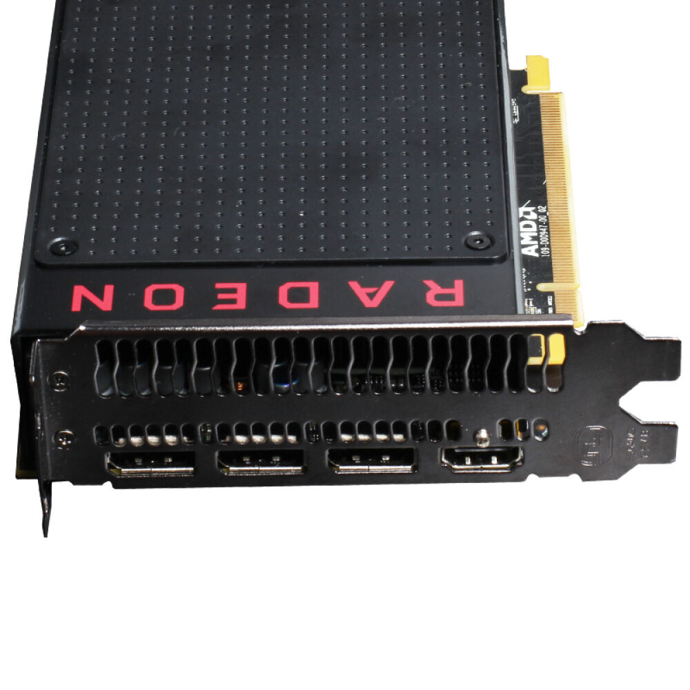
Vega GPU announced with some details, HPC so far

CSI_PC

2[H]4U
Joined
Apr 3, 2016
Messages
2,193
Just released info.
Note: the MI25 is 25TFLOPs FP16, sure this will catch some out as its FP32 is 12.5TFLOPs.

Looks like 1st set of info is based upon HPC world rather than Prosumer or PC Gaming, however that does not necessarily mean it will launch 1st (may do though).
Another aspect, looks like it may be a large-ish die Vega (fits in with what I have mentioned in other threads), still no clarification on core count (full or cut size for smaller GPU).
If it was a small die Vegax2 then FP32 TFLOPs would be higher, and more notably the MI8 would be a single die Vega but it is not.
Looks like Vega is HBM only to me as well, just like Fiji (not being critical just something to consider when discussing gaming or Prosumer).

Where it fits against Nvidia will be interesting as there is no full overlap between each of them; although MI25 is crown of FP32/FP16 Nvidia seems to think the move is towards wanting dedicated GPUs and nodes for training or inference where Nvidia is now pushing Int8, still feel Nvidia missed a point but it has pros/cons for both manufacturers' approach.
The Vega GPU seems focused on FP32/FP16, while Nvidia broaden their selection to be FP64/FP32/FP16 with the P100 or FP32/Int8 (4x) with the P40 and Titan Pascal.
http://videocardz.com/64677/amd-ann...erator-radeon-instinct-mi25-for-deep-learning

Worth noting the 1st 2 cards do not say Vega and are Fiji and smaller model is Polaris, this is what WhyCry reports.
Also regarding Nvidia as a reference the P100 is cheaper than the Tesla P40 (this is Nvidia's top FP32 card but without FP16 and 4xInt8 functions instead), the P100 strength is its high FP64 with good FP32 and FP16 - this figure is influenced by whether it is PCIe (model has slightly lower numbers) or NVLINK.

Edit:
Going back reading WhyCry article, seems he has Nano and Polaris wrong way round.
Cheers
 
Last edited:
300W for the first one. So pretty much 250W for consumer confirmed.

6 is Polaris, 8 is Fiji.
 
Last edited:
300W for the first one. So pretty much 250W for consumer confirmed.

6 is Polaris, 8 is Fiji.
Also I think the naming of the HPC card is going to catch a lot of normal consumers-gamers out, you can tell by its naming that it is really designed for Deep Learning as they focus the name on FP16 performance and not its FP32.
If it had 4xInt8 functions with associated accelerated performance I think Nvidia could had been in trouble against this card, that said it could still pose a reasonable challenge in setups that are more general-mixed Deep Learning nodes-GPUs but importantly AMD still needs to catch up on the software-platform side to truly compete.
Cheers
 
Last edited:
So the mi25 is dual gpu? I'm confused by the clock rates.

Call me a Patty pooper but I don't believe the 1500mhz haha

Lemme check b3d
 
Interesting if that is the case (x2 polaris) Vega is dead in the water.


Apologies for linking to that foul place but someone translated from PCGH
 
So as expected Vega can only compete with GP104. But at much higher power draw.

Expect average performance to fall in between 1070 and 1080 while using 250-300W.

DOOM and 4K is a best case scenario by far.
 
Last edited:
I don't like that x2 packed math, right now it sounds like 2 GPU's. But what ever packed math means, it could be 2x fp16.....
 
So the mi25 is dual gpu? I'm confused by the clock rates.

Call me a Patty pooper but I don't believe the 1500mhz haha

Lemme check b3d


300 watts yeah they can hit 1500mhz..... Most likely pushed way up in the power envelope ranges again too.
 
I doubt the clock is 1500. More like Polaris type clocks.
 
Just something as a pointer. if Vega scores 66.
get
 
AMD should have let ATI crash and burn. Biggest mistake they ever made was buying that company.
 
sub-1080 performance for 1.4x the power? Sign me up!
More like mixing and matching numbers there. I'd say we're looking at two distinctly different products. Only way it makes sense to be a bit faster than GP104 at gaming and 30% faster than P100 at deep learning. That would mean AMD managed 25% higher FP16 performance with 30% less bandwidth than P100. More likely is a Vega10 built like a Nano outperforming GP104. Say 1080 performance in 175W. Worth noting that 66FPS was in a sealed case with horrible airflow and likely throttling. Then a dual die on interposer design outperforming P100. Or they demoed both Vega 10 and 11.
 
More like mixing and matching numbers there. I'd say we're looking at two distinctly different products. Only way it makes sense to be a bit faster than GP104 at gaming and 30% faster than P100 at deep learning. That would mean AMD managed 25% higher FP16 performance with 30% less bandwidth than P100. More likely is a Vega10 built like a Nano outperforming GP104. Say 1080 performance in 175W. Worth noting that 66FPS was in a sealed case with horrible airflow and likely throttling. Then a dual die on interposer design outperforming P100. Or they demoed both Vega 10 and 11.

That's rather optimistic to put it mildly.

And the case is a Corsair Air 240. To say it got bad airflow compared to the average case is quite pushing it. Also why would AMD setup something so it throttled. And dont tell me its to keep the information secret from Nvidia, because that's not the case.
 
More like mixing and matching numbers there. I'd say we're looking at two distinctly different products. Only way it makes sense to be a bit faster than GP104 at gaming and 30% faster than P100 at deep learning. That would mean AMD managed 25% higher FP16 performance with 30% less bandwidth than P100. More likely is a Vega10 built like a Nano outperforming GP104. Say 1080 performance in 175W. Worth noting that 66FPS was in a sealed case with horrible airflow and likely throttling. Then a dual die on interposer design outperforming P100. Or they demoed both Vega 10 and 11.

Sorry but why are we comparing Tom's DOOM numbers to this '66 fps' figure? Where did 66 fps come from?

Doom has no built in benchmark, all these comparisons are useless.

Anarchist4000 what makes you think it's two dies
 
66FPS in 4K is from a video floating around from someone who was there.

what makes you think it's two dies
Just the physics of it. So 1.3x divided by 0.7x = 1.85. That would make it 85% more bandwidth efficient than P100 on deep learning if that 512GB/s number is accurate. On compute which doesn't benefit from compression. In theory with an even smaller die if these things are going to get stuck on interposers with Zen. Going from Polaris 10, they'd have managed 2.6x the die size for maybe double the performance. All while using HBM2 to save power in addition to any architectural upgrades. That's absolutely horrific scaling that only applies to a game they've historically performed well in if true. If Polaris 10 and GP106 have comparable die sizes and performance, I'd expect a Vega 10 with theoretically double the die size of GP104 and better ram to be well ahead. Only explanation I can think of why it outperforms the equivalent of Titan XP (P100) on compute, yet barely surpasses GP104 in gaming. The doom numbers are pretty rough, but reasonably good data from which to extrapolate.
 
66FPS in 4K is from a video floating around from someone who was there.


Just the physics of it. So 1.3x divided by 0.7x = 1.85. That would make it 85% more bandwidth efficient than P100 on deep learning if that 512GB/s number is accurate. On compute which doesn't benefit from compression. In theory with an even smaller die if these things are going to get stuck on interposers with Zen. Going from Polaris 10, they'd have managed 2.6x the die size for maybe double the performance. All while using HBM2 to save power in addition to any architectural upgrades. That's absolutely horrific scaling that only applies to a game they've historically performed well in if true. If Polaris 10 and GP106 have comparable die sizes and performance, I'd expect a Vega 10 with theoretically double the die size of GP104 and better ram to be well ahead. Only explanation I can think of why it outperforms the equivalent of Titan XP (P100) on compute, yet barely surpasses GP104 in gaming. The doom numbers are pretty rough, but reasonably good data from which to extrapolate.

Isn't GP100 ~20tflops fp16?

As far as bandwidth efficiency is concerned I'm not sure its directly comparable because gp100 is a DP chip and there must be headroom for mixed 32/64 operation.

On the other hand I agree it cannot be a 600mm die if it's only 64CU like Fiji.

I'm much more inclined to believe it's two low clocked chips rather than one 1500mjz chip frankly
 
Sorry but why are we comparing Tom's DOOM numbers to this '66 fps' figure? Where did 66 fps come from?

Doom has no built in benchmark, all these comparisons are useless.

Anarchist4000 what makes you think it's two dies

Personally I still think it is a single die and the cut version, with more cores releasing later on the die; same with GP102 1st released with reduced SM-cores and then later full as the P40.
12.5 TFLOPs FP32 is painfully low for a dual Vega die, it would mean each die has less performance than Fiji, and critically less performance than the S9300 which is a 2xFiji card (that is 13.9 TFLOPs FP32 at 300W and that is 28nm).
But me and Anarchist agree to disagree about this in another thread :)
Cheers
 
Last edited:
I would not read too much into its game performance, really surprised it is even being tried with such.
Never saw the P40 used with games.
Both of these are really accelerators rather than game GPUs.

Cheers
 
I would not read too much into its game performance, really surprised it is even being tried with such.
Never saw the P40 used with games.
Both of these are really accelerators rather than game GPUs.

Cheers
If that is the case then AMD really screwed the pooch with their marketing again.
 
Isn't GP100 ~20tflops fp16?

As far as bandwidth efficiency is concerned I'm not sure its directly comparable because gp100 is a DP chip and there must be headroom for mixed 32/64 operation.

On the other hand I agree it cannot be a 600mm die if it's only 64CU like Fiji.

I'm much more inclined to believe it's two low clocked chips rather than one 1500mjz chip frankly
Depends upon whether NVLUNK or PCIE, and worth remembering it is a powerful double precision compute card as well.
As NVLINK it doubles as: 5.3 FP64, 10.6 FP32, 21.2 FP16.
For PCIe it is 4.7 FP64 and then double from that.
However what P100 and the Vega is missing accelerated Int8 functions for inferencing (depends how well Int8 is taking off but seems the direction it is going).
The P40 has no FP64 as such, but 12 FP32 and 47 TOPs (accelerated Int8 packed functions); so FP16 is 2xpacked into FP32 cores for GPUs that support it (P100 and MI25), while Int8 is 4xpacked into FP32 cores acceleration for those that support it (P4,P40,Titan Pascal).
I use the term accelerated as the context is about natively doing the maths, rather than just using the cores as a container (which some of the previous gen could do pretty well).
Cheers
 
Last edited:
If that is the case then AMD really screwed the pooch with their marketing again.
Yeah all it will do is confuse everyone and look at its games performance, which does not correlate well with what one would expect from a gaming GPU with 12.5 TFLOPs FP32 performance.
Cheers
 
12.5 TFLOPs FP32 is painfully low for a dual Vega die, it would mean each die has less performance than Fiji, and critically less performance than the S9300 which is a 2xFiji card (that is 13.9 TFLOPs FP32 at just under 300W).
Theoretical performance, not real performance. Polaris for example sacrificed some compute units to double all the cache sizes. Why the initial estimates were all off as everyone assumed 2560 cores. I haven't seen anything to indicate Vega isn't half rate FP64 either, so a direct comparison to P100 may be warranted. Cazziro had half rate FP64 for an APU from last generation. We could be looking at a Vega10 with significantly less than 4096 cores, say ~3000. In that situation a dual V10 would be reasonable. If V11 were the big chip that could be the 4k core part.
 
Theoretical performance, not real performance. Polaris for example sacrificed some compute units to double all the cache sizes. Why the initial estimates were all off as everyone assumed 2560 cores. I haven't seen anything to indicate Vega isn't half rate FP64 either, so a direct comparison to P100 may be warranted. Cazziro had half rate FP64 for an APU from last generation. We could be looking at a Vega10 with significantly less than 4096 cores, say ~3000. In that situation a dual V10 would be reasonable. If V11 were the big chip that could be the 4k core part.
Well it is all theoretical, AMD's latest announcement is theoretical figures calculated same way as before probably by the same engineers :)
If it had any notable FP64 it would had been in the release info, definitely would not had been forgotten, looks to be the same situation as Fiji to me with regards to FP64.
And remember for Nvidia to do that it required a 600mm2 die, they get better performance out of their P40/GP102 that is 471mm2 by having the minimum DP possible.
Let alone the impact DP has on power demand/TDP.

Cheers
 
Last edited:
A little frustrating having the same conversation on two forums but we could entertain the possibility of a 6SE config with 7 CUs each, 4608 total, this would require a more modest 1350mhz to meet their performance numbers
 
I'd also like to add, despite this inevitably leading to me being called an anti-amd troll, what's with that performance chart? Fiji on par with Pitan X? I understood it to be a standard 32b SGEMM benchmark, what's up with that?
 
Well it is all theoretical, AMD's latest announcement is theoretical figures calculated same way as before probably by the same engineers :)
If it had 2:1 FP64 that would had been in the release info, definitely would not had been forgotten.
And remember for Nvidia to do that it required a 600mm2 die, they get better performance out of their P40/GP102 that is 471mm2 by having the minimum DP possible.
Let alone the impact DP has on power demand/TDP.

Cheers

Nvidia uses independent FP64 units as of now, whereas AMD was using FP32 vector lanes in pairs to compute 64b, afaik details of the implementation are not available but their FP32 units must support extra bits as it is IEEE compliant
 
Nvidia uses independent FP64 units as of now, whereas AMD was using FP32 vector units in pairs to compute 64b, afaik details of the implementation are not available but their FP32 units must support extra bits as it is IEEE compliant
Worth remembering Fiji cannot do FP64, which was one reason they kept older gen just like Nvidia that could not do FP64 with Maxwell.
It was 1/16th ratio for Fiji I think (needed Hawaii GPUs if FP64 a requirement), Nvidia was 1/32 in Maxwell (required Kepler and either K40 or K80 for FP64).

Cheers
 
Back
Top