NVIDIA White Paper Details Multi-Chip Module GPU Design

Megalith

24-bit/48kHz
Staff member
Joined
Aug 20, 2006
Messages
13,000
Packing more transistors into a monolithic GPU won't be feasible for much longer, and a new white paper from NVIDIA and university researchers suggest that the company may look to multi-chip module designs to get around the limitation of Moore’s Law. Proposed is a strength-in-numbers approach: multiple GPU modules would be connected using advanced, high-speed input/output protocols to efficiently communicate with each other, and this would allow for less complex (and presumably cheaper) GPU modules compared to a monolithic design.

Without either switching to a multi-chip module design or coming up with an alternative solution, Nvidia warns that the performance curve of single monolithic GPUs as currently constructed will ultimately plateau. Beyond the technical challenge of cramming more transistors into smaller spaces, there is also the cost to consider, both in terms of technical research and reduced die yields. Whether or not an MCM design is ultimately the answer, Nvidia thinks it is at least worth exploring. One thing that Nvidia mentions in its paper is that it's difficult to scale GPU workloads on multi-GPU systems, even if the scale will on a single GPU.
 
Proposed is a strength-in-numbers approach: multiple GPU modules would be connected using advanced, high-speed input/output protocols to efficiently communicate with each other, and this would allow for less complex (and presumably cheaper) GPU modules compared to a monolithic design.
Sounds like what AMD is doing with Ryzen.
 
We will just have to hope that it won't be something that programmers have to setup on their side. We all know how long it took for multi-core processors to get used.
They will figure something out... they always do...
 
I thought voodoo already tried that?

This is aimed at improving compute density while lowering costs (think supercomputers). It assumes that smaller dies are much easier to make than massive V100 dies.

The only issue is the interconnect, and the software to drive things. This looks like i uses HBM stacked ram, which is the same thing they use on V100. But I'm not sure what the interconnect is.

They seem to have gotten NVLINK working effectively, so maybe they'll knock this one out-of-the-park?

But it could mean a change from massive compute dies in the near future.
 
Are we going to go back to specialized chips for different jobs? Perhaps a central chip to assemble the framebuffer, with separate chips for lighting, texturing, and wireframe?

SLI/crossfire is incredibly inefficient with regards to memory, so just making it a multichip SLI config is not going to work, unless they start loading GPUs with 32-64GB of memory.
 
I guess it depends if they can come up with a really efficient/fast bus to connect the moduals.
 
  • Like
Reactions: Nenu
like this
yes 3dfx tried this ..i still have a card that tried it .. a VOODOO 5 5500 ..and an nvidia Geforce 2 GTS card beat it..

then Nvidia bought 3 d fx ..hmm

spent $400 on my vodoo card , then 400 on my GTS card .. GO Nvidia !

keep me buying shit that gets outdated in a 6 month period ! LOL ..thats how PC's have always worked
 
Navi scalable architecture was what I first thought of too when reading this. They already have Infinity Fabric, designed for CPU's and GPU's, working in production silicon (for Ryzen) so will be interesting to see the Navi implementation.
 
I thought voodoo already tried that?

And AMD and NVidia. It is essentially all just CF/SLI on a a single card.

It has never really been much better than CF/SLI on separate cards.

One big issue is the waste of memory as each chip ends up talking to it's own memory pool.
 
I see this being more like threadripper then CF/SLI.

There are cars that are basically two separate GPU's glued together with built in SLI bridge - this is multiple modules all interconnected.

If they can come up with Ryzen like cores with a good bus I could see GPU's changing considerable - a PCIE board with a modular processor section and dimm type slots for the ram. Kinda a mini motherboard. Could be done other ways as well of course.

Threadripper is kind of like CF/SLI for a CPU. There isn't much logical difference. It's is simply a question of how fast the interconnects are, and how much more Bandwidth hungry GPUs are vs CPUs.

Each CPU block in threadripper has it's own memory controller and connects to it's own memory pool.

It will be interesting what they say about populating memory channels. But I am betting there will be strong admonishments to populate threadripper core memory even ahead of filling in memory channels.

So far for GPUs, the interconnects haven't been fast enough to share memory pools, even if the interconnects are fast, you would be using the memory controller on the other GPU to access it's memory pool, creating contention with it's own calls.

I see no easy solution for sharing GPU memory in multi-chip solutions.
 
And AMD and NVidia. It is essentially all just CF/SLI on a a single card.

It has never really been much better than CF/SLI on separate cards.

One big issue is the waste of memory as each chip ends up talking to it's own memory pool.
I thought it was more like the days when we slaped two dies right next to each other on the same chip and called it dual core. so they'd share a cache and memory like a normal chip. You know the sweet Pentium D days
 
I thought it was more like the days when we slaped two dies right next to each other on the same chip and called it dual core. so they'd share a cache and memory like a normal chip. You know the sweet Pentium D days

Are we going back to an external Northbridge with memory controller in it?

GPUs are memory bandwidth hogging beasts, you would end with bus contention and effectively half the bandwidth if they tried to share a pool of memory.

It will be a big breakthrough if someone comes up with a way to effectively share a GPU memory pools, but so far they are independent.
There are ways to minimize clashes. But just like a CPU, there will be caches. And Navi is supposed to implement a new type of memory architecture. And I have been playing with the "hypothetical" function blocks, and I think I have a pretty good idea how they will access said memory with a minimal of conflicts.

So yes, it is possible. But it's unlike anything that is out there today. The secret will be in the scheduler and the loader for each GPU.
 
I doubt we will ever see anything like this in gaming environment in a long long time if at all.
 
Different animals, I understand, but the Ryzen model won't work for GPU?

You're likely right (you're privy to more inside info than we are), but it sure would be fascinating if you are wrong - because if you are wrong, and the people who say this is already what's in Navi are right, it would likely mark the first time in quite a while that AMD would have a head start over NVidia in terms of technology and be a game changer (provided something like this ends up working awesome for gaming).
Actually I hope I am wrong.
 
I guess it depends if they can come up with a really efficient/fast bus to connect the moduals.
Yep.
A very high freq interconnect will help greatly.
While its max bandwidth could eclipse data transfer requirements (ie wont be necessary), the reduced latency would have a large effect bringing the GPUs closer to a single die design.
 
I did a quick skim through the paper. This is more about working for compute loads, than Graphics loads.

IMO, the problem for Graphics, that I brought up before remains. You are essentially dividing up your effective memory by the number of GPU chips you have, just like you do with CF/SLI.

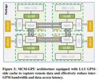
Because each GPU has it's own pool of memory and they are connected in a crossbar interconnect NUMA arrangement to get info from other pools if you need it:
MCMGPU.PNG

A lot of the work in the paper is on minimizing the use of the interconnects by keep data local to the GPU. But it is all for Compute loads, and they provide several benchmarks. They don't address graphics loads at all.

For Graphics (Gaming), you relying much more heavily on that memory for textures, and it is likely impossible to spread this out, so you need to duplicate texture memory in each pool, effectively limiting memory to the amount in each pool

So a 16GB 4 way MCM GPU would act more like a monolithic GPU with 4GB of Memory.

I don't think there is an easy way around this problem for graphics.

But if memory is cheaper than the difference between two smaller chips and one bigger chip, you still might do this...

As I stated before, there are ways around this to minimize the hit. It would drastically change how things are handled today. You would predict ahead of time which textures are going to be rendered by which tile and effectively feed that into a sub processor into a cache. This is where a clever on chip scheduler comes into play. There's a whole host of tricks I've been working up on paper for a couple months now to improve efficiency. This includes a new type of concurrent memory access on a ringed bus, which would require a new type of memory interconnect.

But for this to be effective the scheduler has to be wicked fast compared to the tile renderer to keep the sub processors busy. So if before the draw call to the sub processor, if you have say 10 cores, then the scheduler has to be able to issue a new draw sub call in the 1/10th the time that is takes the sub processor to render the tile.

But it's interesting the white paper hit all the points I wrote about to the benefits of a similar architecture.
 
Last edited by a moderator:
I dont know the nitty-gritty hard ware end like many here do...

Is there a way to set up multiple DMA connects to a block of ram, like a frame buffer? So each 'cell' does its own work and concurrently writes to the frame buffer?

Instead of tearing when things are running slow you'd see whole blocks of the screen looking out of phase... kinda weird looking I bet.
 
I did a quick skim through the paper. This is more about working for compute loads, than Graphics loads.

IMO, the problem for Graphics, that I brought up before remains. You are essentially dividing up your effective memory by the number of GPU chips you have, just like you do with CF/SLI.

Because each GPU has it's own pool of memory and they are connected in a crossbar interconnect NUMA arrangement to get info from other pools if you need it:
View attachment 29763

A lot of the work in the paper is on minimizing the use of the interconnects by keep data local to the GPU. But it is all for Compute loads, and they provide several benchmarks. They don't address graphics loads at all.

For Graphics (Gaming), you relying much more heavily on that memory for textures, and it is likely impossible to spread this out, so you need to duplicate texture memory in each pool, effectively limiting memory to the amount in each pool

So a 16GB 4 way MCM GPU would act more like a monolithic GPU with 4GB of Memory.

I don't think there is an easy way around this problem for graphics.

But if memory is cheaper than the difference between two smaller chips and one bigger chip, you still might do this...


Really the only way around this is if the control silicon can communicate with each other without any limitations. Once that is achieved, memory pooling will be easy to accomplish. So the cache has to be large enough to cover the interconnect latency. And the way current chips are set up, that would L1 cache, not L2 or global.

We already see on Ryzen the interconnect can't cover that ground, on a CPU which its needs are much less than a GPU. So lots more work will need to be done.
 
its possible. We already see the cache size increase in Volta.
 
its possible. We already see the cache size increase in Volta.

I haven't seen cache specs on Volta, but it is likely trivial in comparison to Texture needs.

We will see dual GPU graphics cards no doubt, which we have seen nearly every generation since the Voodoo 5.

I doubt we will see quad GPU graphics card in the foreseeable future.
 
hmm did I just give something away lol:hungover: this is what happens when I drink to much the night before lol.
 
Threadripper is kind of like CF/SLI for a CPU. There isn't much logical difference. It's is simply a question of how fast the interconnects are, and how much more Bandwidth hungry GPUs are vs CPUs.

Each CPU block in threadripper has it's own memory controller and connects to it's own memory pool.

It will be interesting what they say about populating memory channels. But I am betting there will be strong admonishments to populate threadripper core memory even ahead of filling in memory channels.

So far for GPUs, the interconnects haven't been fast enough to share memory pools, even if the interconnects are fast, you would be using the memory controller on the other GPU to access it's memory pool, creating contention with it's own calls.

I see no easy solution for sharing GPU memory in multi-chip solutions.
Ehh, it's a bit different. Ryzen/Threadripper were built around the fabric architecture, whereas CF/SLI is just allowing two separate entities talk/work in tandem. Even the smallest Ryzen/Epyc CPU has the fabric, whereas in the other scenario you'd just have a single GPU.
 
Ehh, it's a bit different. Ryzen/Threadripper were built around the fabric architecture, whereas CF/SLI is just allowing two separate entities talk/work in tandem. Even the smallest Ryzen/Epyc CPU has the fabric, whereas in the other scenario you'd just have a single GPU.

Logically it isn't much different. You have independent units, with independent memory pools, with interconnects between them.

The devil is in the details. While NUMA is suitable for CPU use, it really isn't for Graphics. This paper isn't really about graphics at all.
 
Back
Top