Nvidia announces RTX 2050 mobile GPU (not a typo)

NattyKathy

[H]ard|Gawd
Joined
Jan 20, 2019
Messages
1,483
I'm honestly at a loss for words.
geforce-ampere-rtx-2050-social-twitch-1200x480-1.jpg


Wait, no, I do have a few words.
WHAT. THE. HELL. IS. GOING. ON. AT. NVIDIA.

It's based on GA107.
GA107
They're branding Ampere chips as RTX 2000 now. This is not a drill.
That's the last straw, I'm pretty sure I feel a brain aneurysm coming on.
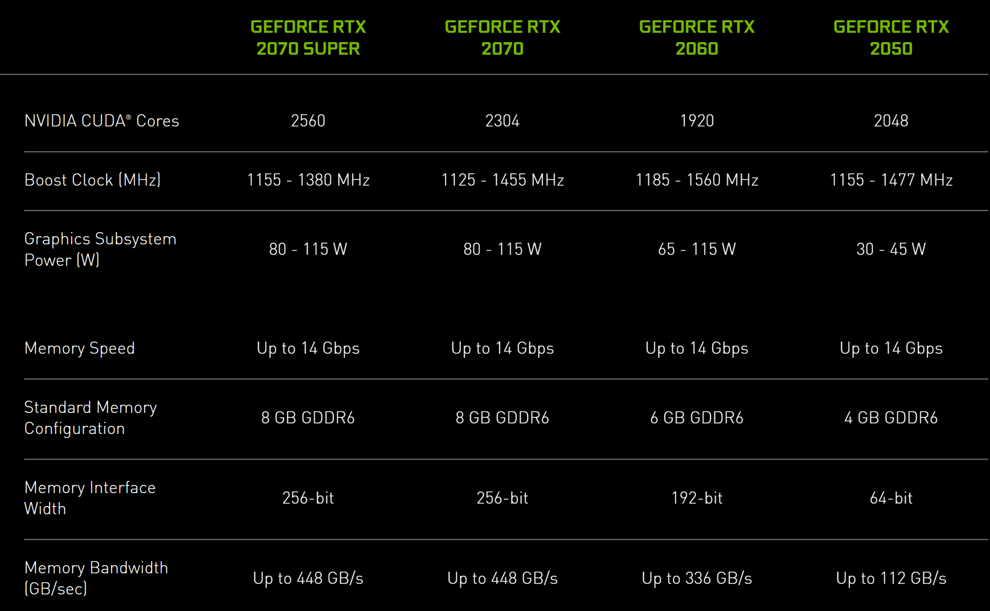
NVIDIA-RTX-2050-GPU.png
 
leftovers?! they are re-releasing desktop cards too. there was that post about them stopping 3000 production so maybe these were still kicking around, idk. are the 2000 and 3000 produced at different plants? if so maybe they only have access to the 2000 one, again, idk.
 
I'm honestly at a loss for words.

View attachment 422858

Wait, no, I do have a few words.
WHAT. THE. HELL. IS. GOING. ON. AT. NVIDIA.

It's based on GA107.
GA107
They're branding Ampere chips as RTX 2000 now. This is not a drill.
That's the last straw, I'm pretty sure I feel a brain aneurysm coming on.


Are you sure these are Ampere chips, and not leftover Turing chips, like the 12GB 2060's that are due out any day now? I know you posted that they are GA107's, but could that be a mistake in the source?

I had assumed they were either leftover Turing chips, or newly manufactured Turning chips because they can still be manufactured on older 12nm processes for which the demand is not as insane as 7nm and 8nm processes.

My understanding right now is that the supply limitations are all in 7nm and 8nm fabrication. If you still want to manufacture something in 12nm or older capacity and scheduling are A LOT easier.
 
leftovers?! they are re-releasing desktop cards too. there was that post about them stopping 3000 production so maybe these were still kicking around, idk. are the 2000 and 3000 produced at different plants? if so maybe they only have access to the 2000 one, again, idk.
All consumer Ampere is on Samsung 8nm and all Turing is on TSMC 12nm. Or do you mean the packaging part? That I have no idea about.
Re-releasing a TU106 RTX 2060 actually kind of made sense since it's on an older process that's less constrained but this makes no sense at all.
 
All consumer Ampere is on Samsung 8nm and all Turing is on TSMC 12nm. Or do you mean the packaging part? That I have no idea about.
Re-releasing a TU106 RTX 2060 actually kind of made sense since it's on an older process that's less constrained but this makes no sense at all.
no i was thinking what zara and you said.
they are still great cards just no rtx, which is not that big of a deal for 90%+ of gamers, imo.
 
Are you sure these are Ampere chips?

I had assumed they were either leftover Turing chips, or newly manufactured Turning chips because they can still be manufactured on older 12nm processes for which the demand is not as insane as 7nm and 8nm processes.

My understanding right now is that the supply limitations are all in 7nm and 8nm fabrication. If you still want to manufacture something in 12nm or older capacity and scheduling are A LOT easier.
I also find it exceedingly difficult to believe these are Ampere too given the production bottlenecks on Sammy 8nm, but that's what Videocardz says and 2048 CUDA core is a typical GA107 config, not a TU106 one as is the 64-bit memory bus.

Hence my current disoriented mental state
 
I also find it exceedingly difficult to believe these are Ampere too given the production bottlenecks on Sammy 8nm, but that's what Videocardz says and 2048 CUDA core is a typical GA107 config, not a TU106 one as is the 64-bit memory bus.

Hence my current disoriented mental state

Hmm. Odd.

I mean, it is not uncommon for GPU manufacturers to go over their old inventory and re-bin chips that previously did not make higher bins to see if they have enough to release a lower end model, but if that is what they did with their inventory of Ampere chips, the 2050 naming convention seems very odd.

Maybe they just didn't feel right releasing something that performed that poorly under the 30xx name?

I mean, it hasn't stopped them before. There are 710's and 720's out there, but who knows.

Some consistency in naming would be appreciated.

Also, NEVER naming two different products the same thing would also be greatly appreciated.

I guess we will have to wait to see the official releases from Nvidia.

It is not unheard of that early information like this might be wrong.
 
no i was thinking what zara and you said.
they are still great cards just no rtx, which is not that big of a deal for 90%+ of gamers, imo.
GA107 does have RT and Tensor cores- not enough to 'trace worth a damn but they support DLSS at least, which a 16CU Ampere card with 64-bit memory bus will definitely need to get good performance at any HD resolution!
 
Also,

There is more here that doesn't make sense. Why utilize a 2048 core chip for this, only hamstring it with a 64bit memory bus?

Seems like there would be ample opportunity to use lower core count silicon in this application.

It seems wasteful. There is definitely something weird going on here.
 
Nvidia has been using "odd" standards in the way that they name their mobile GPUs for a long time now.

For example, in 2012 I got a laptop that had a GT630M GPU. On the desktop, 500 series GPUs were Fermi, 600 series GPUs were Kepler. Fermi cards were cut off from the current driver in 2018, while Kepler cards were only cut from the current driver a few months ago (late 2021). But even though the GPU in the laptop is labeled as 600 series, it's actually based on Fermi (desktop 500 series equivalent). That means the GT630M was cut off from the current driver in 2018 also. So their naming scam literally cost me 3 years worth of GPU driver updates.
 
Also,

There is more here that doesn't make sense. Why utilize a 2048 core chip for this, only hamstring it with a 64bit memory bus?

Seems like there would be ample opportunity to use lower core count silicon in this application.

It seems wasteful. There is definitely something weird going on here.
I agree, something exceedingly odd here. Why not call it a 3040? I have never seen a downward rebrand before. Ever. Unless G92 counts but that was way less wacky than this malarkey.
All evidence points to it being GA107 though, despite that being utterly nonsensical.
TU106 won't hit those clock speeds in a 30-45W envelope (says a lot)
32SM isn't a core config we've seen with TU106 yet (doesn't say much)
64-bit memory bus would be a shitshow on TU106 (says a lot)

Hmm. Odd.

I mean, it is not uncommon for GPU manufacturers to go over their old inventory and re-bin chips that previously did not make higher bins to see if they have enough to release a lower end model, but if that is what they did with their inventory of Ampere chips, the 2050 naming convention seems very odd.

Maybe they just didn't feel right releasing something that performed that poorly under the 30xx name?

I mean, it hasn't stopped them before. There are 710's and 720's out there, but who knows.

Some consistency in naming would be appreciated.

Also, NEVER naming two different products the same thing would also be greatly appreciated.

I guess we will have to wait to see the official releases from Nvidia.

It is not unheard of that early information like this might be wrong.
I would love for NV to be consistent with their naming. That RTX 3050 4G vs 8GB thing is cringe.
The upcoming 12GB "3080" thing is atrocious too.
Call different things different names so we know they're different without digging through spec sheets. FFS, NV.
 
Nvidia has been using "odd" standards in the way that they name their mobile GPUs for a long time now.

For example, in 2012 I got a laptop that had a GT630M GPU. On the desktop, 500 series GPUs were Fermi, 600 series GPUs were Kepler. Fermi cards were cut off from the current driver in 2018, while Kepler cards were only cut from the current driver a few months ago (late 2021). But even though the GPU in the laptop is labeled as 600 series, it's actually based on Fermi (desktop 500 series equivalent). That means the GT630M was cut off from the current driver in 2018 also. So their naming scam literally cost me 3 years worth of GPU driver updates.
Yeah, NV has been on that BS for a long time now unfortunately :-/

What makes this different and is causing my brain physical pain is that this isn't rebranding older low-end cards as new low-end cards; they're rebranding a newer card (3050) as an older one.
 
Considering the RTX 3050 mobile (the non TI) was almost identical (GA107, etc...) but a 128 bit bus is there anything special to this new ?

Or simply we did not register that it was the case when that was release last May ?

I also find it exceedingly difficult to believe these are Ampere too given the production bottlenecks on Sammy 8nm
If we would know the die size it could make a lot of sense, it is apparently 160mm to 180mm2, a 3050TI/3060 on the older GA106 was 276 mm2, the 3070TI mobile on the GA104 ampere gpu was 392mm2

They can I imagine make much more of those for any better chips that is not made. In the current environment no product make sense or not without taking into account how many you can make relative to other options I feel like.
 
Considering the RTX 3050 mobile (the non TI) was almost identical (GA107, etc...) but a 128 bit bus is there anything special to this new ?

Or simply we did not register that it was the case when that was release last May ?


If we would know the die size it could make a lot of sense, it is apparently 160mm to 180mm2, a 3050TI/3060 on the older GA106 was 276 mm2, the 3070TI mobile on the GA104 ampere gpu was 392mm2

They can I imagine make much more of those for any better chips that is not made. In the current environment no product make sense or not without taking into account how many you can make relative to other options I feel like.
This indeed looks to be just a 3050 mobile with the memory bus cut in half, the issue is that it would have made more sense to call it a 3040 than 2050. RTX 3050 launch didn't confuse people because it was the next step down in the product stack and makes perfect sense from a segmentation standpoint.

Where do you see 160-180mm^2 die size listed for RTX 2050? That would be in line with GA107...

Pretty sure 3050 and 3050Ti are both GA107 and 3060 is the only mobile GA106 card.
 
Where do you see 160-180mm^2 die size listed for RTX 2050? That would be in line with GA107...
I found nothing else than rumors /expectation from a google search:
https://hitechglitz.com/intel-arc-a...idias-ga104-dg2-128-almost-halved-from-ga106/

the issue is that it would have made more sense to call it a 3040 than 2050
I think we have not seen a 40 version of a card in a very long time, I imagine there is a naming strategy here, one not associate that level of performance to the 3xxx brand, while for the 128 bit ampere it was ok.
 
Looks like a pretty easy OEM replacement for the dwindling supply of the 1650s that are in just about every budget gaming laptop under the sun right now.
Looking at their specs side by side they may even be pin compatible.

But the existing 1650 laptop parts are based on the TU117 chip and it's looking like the 2050 is going to be based on the TU106, so assuming they are priced about the same I could see this easily being paired up with the Intel 12'th gen mobile parts for launch in Q2, 2022.
 
Last edited:
It just Nvidia spinning up old unused nods to relieve the shortages. These are perfectly fine for lower laptops.
 
wondering how this stacks up to the 1650 that is in just about every budget gaming laptop under the sun right now.
1650 will be about the same I think. Maybe a little faster depending on how bad GA107 reacts to 64-bit memory bus. This abomination may have better perf/W though and does support DLSS.
 
It just Nvidia spinning up old unused nods to relieve the shortages. These are perfectly fine for lower laptops.
This doesn't look to be an old node though, that's what's so odd. All info currently available points to these being GA107 Ampere- same 8nm Samsung chip as RTX 3050. Hence everyone's befuddlement. Yet Another TU106 would be one thing but this is truly off the rails if it really is GA107 RTX 2000
 
1650 will be about the same I think. Maybe a little faster depending on how bad GA107 reacts to 64-bit memory bus. This abomination may have better perf/W though and does support DLSS.
The 1650 has half the core count, half the transistors, has a slightly faster boost (cooling dependent) but a slower base, and almost half the memory speed of the proposed 2050. Looks like the 2050 should spank the 1650 pretty handily
 
The 1650 has half the core count, half the transistors, has a slightly faster boost (cooling dependent) but a slower base, and almost half the memory speed of the proposed 2050. Looks like the 2050 should spank the 1650 pretty handily
Maybe, maybe not. 1650 has 8GT GDDR5 on a 128-bit bus whereas this has 14GT GDDR6 on a 64-bit bus so the 1650 actually has slightly more bandwidth. Also, due to the new way NV counts CUDA cores on Ampere, one can't just compare core counts directly, you have to use a multiplier that shifts depending on card class as performance scaling changes as core counts increase. Case in point- RTX 3060 is not that much faster than RTX 2060 despite having twice as many "cores" because the Shader Module count stayed the same and NV just started counting the FP and INT paths as separate cores.
 
Maybe, maybe not. 1650 has 8GT GDDR5 on a 128-bit bus whereas this has 14GT GDDR6 on a 64-bit bus so the 1650 actually has slightly more bandwidth. Also, due to the new way NV counts CUDA cores on Ampere, one can't just compare core counts directly, you have to use a multiplier that shifts depending on card class as performance scaling changes as core counts increase. Case in point- RTX 3060 is not that much faster than RTX 2060 despite having twice as many "cores" because the Shader Module count stayed the same and NV just started counting the FP and INT paths as separate cores.
Yeah, but it wouldn't be unreasonable to see the same sort of performance gain from the 1650 to the 2050 as you would expect to see from going from a 2060 to a 3060. Which assuming it's a new silicon batch would still be a 20'ish percent performance improvement while being cheaper.
But I mean, if I had a choice between an 11th gen Intel paired with a 1650, or a 12'th gen with the 2050 all else being equal the 2050 is going to be an easy choice to make.
oh for sure! This will be the better choice vs 1650, I'm just saying, my expectations are tempered :p
 
I agree, something exceedingly odd here. Why not call it a 3040? I have never seen a downward rebrand before. Ever. Unless G92 counts but that was way less wacky than this malarkey.
All evidence points to it being GA107 though, despite that being utterly nonsensical.
TU106 won't hit those clock speeds in a 30-45W envelope (says a lot)
32SM isn't a core config we've seen with TU106 yet (doesn't say much)
64-bit memory bus would be a shitshow on TU106 (says a lot)


I would love for NV to be consistent with their naming. That RTX 3050 4G vs 8GB thing is cringe.
The upcoming 12GB "3080" thing is atrocious too.
Call different things different names so we know they're different without digging through spec sheets. FFS, NV.
Obfuscation is by design, so less-informed consumers pay a premium for a lesser part. Been happening for awhile.
 
Obfuscation is by design, so less-informed consumers pay a premium for a lesser part. Been happening for awhile.

...and it should be illegal.

Borderline fraudulent if you ask me.

Reminds me of the time I ordered a GT1030 for an htpc. I confirmed in the detailed specifications that it was a GDDR5 version, but actually received a DDR4 version
 
More info, including analysis and preliminary Time Spy scores (in Chinese)

Takeways:

Preliminary RTX 2050 Time Spy GFX score is the same as GTX 1650 notebook (around 3400pts) but if I'm reading it right, the person who wrote the linked post believes shipping parts may score close to 4000pts- this range is about what I would expect for what is ultimately an RTX 3050 that's being intentionally and severely bandwidth bottlenecked.
The RTX 2050 and MX 570 are confirmed to be using GA107 Ampere core
MX550 is using TU117 core
RTX 2050 does support RTX and DLSS
MX 570 does not support RTX or DLSS
Memory will be 11GT/s, 12GT/s, or 14GT/s depending on TGP bracket
RTX 2050 and MX 570 are using the same core and memory bus configuration, the differences being VRAM quantity, and the MX card disabling RT Cores, Tensor Cores, and NVENC.
 
Maybe the performance (due to laptop cooling and power contraints) puts this Ampere chip at below Turing 2060 laptops' performance. So it is just labeled to place it in the lineup in relation to where the performance is.

If you are going to buy a laptop to game on, you want to be sure to do your research on performance plus how that affects heat and battery life.

And if you are buying a laptop for more typical uses, this would probably be a good choice vs onboard intel graphics.
 
Back
Top