[H]oax Debunked]AMD X390 and X399 chipsets diagrams leaked?

CAD4466HK

2[H]4U
Joined
Jul 24, 2008
Messages
2,741
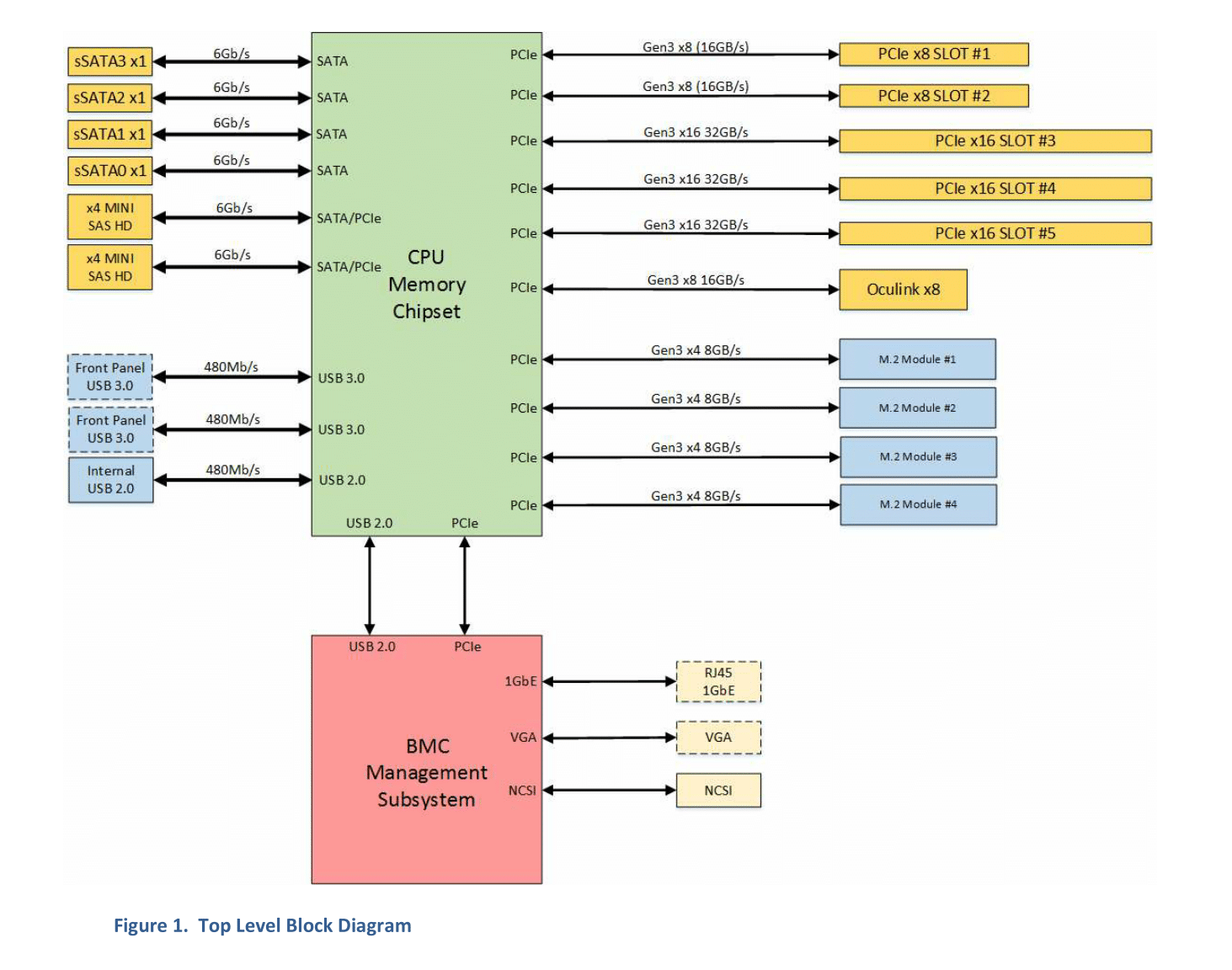
A Reddit user posted few diagrams allegedly showing yet unreleased X399/X390 platforms for AMD’s High-end CPUs. We can’t confirm that these diagrams are real, but we reached out to the original poster for more information. In the meantime, treat this as a rumor.

https://videocardz.com/67594/rumor-amd-x390-and-x399-chipsets-diagrams-leaked

Seems a Chinese site has debunked this leak.
I will let you decide for your selves.

http://www.microsofttranslator.com/BV.aspx?ref=IE8Activity&a=http://www.mykancolle.com/?post=1521


[*]The AMD leak is showing the wrong sockets


[*]It's basically just modify the Intel board to look like AMD leaks


[*]the Intel X299 leaks from the same Chinese guy is also fake, based on last gen server board
[*]What we do know:


[*]X390/X399 exists with Socket SP3/SP4


[*]It will come with 2MCM 16 cores/4MCM 32 cores for X390/X399


AMD-X390-Motherboard.png
AMD-X399-Chipset-1000x922.jpg
AMD-X390-Chipset.png
 
Last edited:
If confirmed true, i might need to wait and see how things are when this one is released.

That looks pretty interesting as a platform to me.
 
Rumors about a higher end workstation platform for AMD's Zen architecture have been floating around for some time now, and while we like to focus on bringing you confirmed news, even we can't ignore them forever. The rumors are really based on these images, and the rest is conjecture at this point, suggesting that X399 for dual socket designs and X390 for single socket designs will be supporting a new AM44 socket. If you like counting PCIe lanes on pictures you'll see that X390 has 44 PCIe lanes (slightly more than Intel's top -E products) as well as Quad Channel RAM. The rumors suggest that these are intended to be used with 16 core 32 thread Zen based CPU's.

If you, like me, have been waiting for a more Workstation-oriented Zen, this might be it. The extra PCIe lanes and Quad Channel RAM are certainly right up my alley, even though I think 16 cores is more than I need. I'd rather have an 8 core part with higher clocks.

As always, take this with a boatload of salt, as the source on this one is Reddit.
 
I was wondering about the SATA config on the X399.
I see 6 xSATA6 and 2xESATA, then I see x2 by the ESATA, does that mean x4 for the ESATA?
And I know usually those can be configured in the BIOS to be SATA, if so this would mean only 10 SATA ports.

If I am incorrect on the x4(leaving only 8)then I should hope they will incorporate some 3rd party SATA chips.
A mobo of this caliber should have at least 10 IMHO, it would make for a great PLEX/storage sever for me if it had more.
I've been eyeballin' the Asrock X99 Extreme 11 that has 18 SATA ports. But that fucker is waaaay out of my price range.
 
  • Like
Reactions: N4CR
like this
I was wondering about the SATA config on the X399.
I see 6 xSATA6 and 2xESATA, then I see x2 by the ESATA, does that mean x4 for the ESATA?
And I know usually those can be configured in the BIOS to be SATA, if so this would mean only 10 SATA ports.

That's the problem with generating rumors based on leaked images. It always involves some guesswork.
 
no idea if diagrams are true or BS, but one thing is sure, it would be stupid of AMD not to release an HEDT part, since most reviews seem to land it on that space, but for it to be worth it, the price needs to be really attractive to increase the market from desktop one, because right now HEDT is a small nich, but that's mostly because of the prohibitive intel pricing.
 
Rather have less cores and higher clocks without the CCX complexes. Also support for higher bandwidth rated memory, 3000+.
Also 2x M.2. PCIE3.0 x4 buses.
 
As cool as it is to see this leaked stuff. I think some of us need to remember these are likely going to be powering $700-800 motherboards. I am interested as I have some clients that may pair something like this with high end workstation 3d cards. However in most of those cases the 16 core Ryzens are likely overkill anyway as the majority of their horsepower is coming from the GPU, cards like AMD 9100s and OpenCL compute.

I am looking forward to seeing how the Server class Monster Ryzens compare though. Interesting leak info if its true.
 
no idea if diagrams are true or BS, but one thing is sure, it would be stupid of AMD not to release an HEDT part, since most reviews seem to land it on that space, but for it to be worth it, the price needs to be really attractive to increase the market from desktop one, because right now HEDT is a small nich, but that's mostly because of the prohibitive intel pricing.

The problem with selling HEDT to compete with Intel's is "What is AMD going to do to increase performance? Are they just selling us more cores and quad channel memory? So much need to change to make a truly fast cpu that's faster than the Kaby Lake IPC wise.
 
What I find the most wrong with these pics is the dual i211 NICs. They should be using the x4 lanes from the X390 for a dual 5Gb or single 10Gb NIC.
 
You don't love the colck, huh? :p

I wouldn't necessarily take that as a sign that it is forged.

Internal engineering documents have typos all the time, especially if they are drafts not ready for formal use.

Yeah, I know. I was just mostly being sarcastic while nitpicking at an obvious, yet minor flaw. However, it did set off a flag none the less. :D

I mean, I just don't know how colck signals operate.:p
 
Those pics have the socket labeled as AM44?

I didn't think that was the name of the workstation socket. Maybe I'm wrong.

Another thing that's curious. I see 1394 internal headers and at least 2 on the back panel. Unless something has changed, I thought 1394 was Firewire and I haven't seen a firewire plug in 10 years.

Basically the "block diagrams" are bullshit.
 
X390 .. Does AMD not realize they use the #90X name elsewhere in their brand? Talk about confusing.
 
I mean, I just don't know how colck signals operate.:p
As the electrons become more and more excited, the colck begins to increase. Additionally, it changes from a very drooping shape, to a long flat one.


More on topic... lol
What I'd be focusing my efforts on is finding Intel or older G34/C34 diagrams to compare with, and make sure it wasn't just something someone made for the lawls (see: hoax).

Things that jump out at me... Zero mention of SAS. Not even a single port, which I find quite odd, personally, but I don't keep up with HEDT/Workstation boards. I just assumed it was a no brainer that they'd have them given they can handle SATA drives as well. Looking around I found this regarding Skylake-EP (click for larger):

It has 4 SATA ports, and then 2 Mini SAS ports (which being serial can be daisy chained for 4 drives each port). Total storage there? 12 drives.
(BTW the 'sSATA' just seems to be some BS Intel marketing lingo as I can't track down any logical reference aside from ones powered by an external secondary SATA chip, which this seems to NOT be.)

The 100 or 101 (did I math them correctly? lol) PCIe 3.0 lanes seem to be pretty comparable to what the proposed RZ2700 is capable of. However, those bandwidths on the Skylake-EP image show PCIe 4.0 speeds, despite saying Gen3 (at least according to the PCIe Wiki page. It states: "v 4.0 = 31.51 GB/s (×16)" and "v 3.x = 15.75 GB/s (×16)", so perhaps even that diagram needs to be taken with a grain of salt?)

Other than that, there's the fact the CPU diagram says "PEG" for the PCIe lanes, which in addition to not one, but THREE references to "colck", makes me more skeptical due to PEG being PCI-express Graphics... and if that's what they were dedicated to, then what are two SSDs (m.2?) and two Gigabit LANs doing there?

Lastly, I'd be curious as to whether Intel has any sort of "design" patent on bifurcated memory banks like what was started with the X58. I can't honestly recall if I've ever seen an AMD based server board with the memory slots split up. With the old Magny-Cours G34 you had two giant blocks of 8 DIMM slots per GPU on those. And the only reason I'd even think it MIGHT be patented is simply due to the fact it's unique. But *shrug*


What I find the most wrong with these pics is the dual i211 NICs. They should be using the x4 lanes from the X390 for a dual 5Gb or single 10Gb NIC.
I'm not sure I can agree with that on account of that x4 PCIe 3.0 lanes going TO the X390 chipset is needed for everything you see connected to it. That means all the USB connections, the SATA ports, those green PCIe lanes are which I can only imagine, for sanity sake, to be PCIe 1.0 seeing as there's so much shit being jammed through that poor 3.0 x4 bridge as it is... Granted, a lot of that will no doubt be like current boards where if X is in use then Y is disabled, but still. One needs to keep in mind that at PCIe 3.0 at x4 link, comes in at just shy of 4GBytes/s of bandwidth. So it's unlikely that the SATA will be disabled, and the theoretical bandwidth of a 10Gbe connection is 1.25GBytes. Two of those could potentially eat up over half of that on their own, nevermind contending with storage transferring.

However, even with 2x 5Gbe or a single 10Gbe, feels like an awful lot to cram down that x4 link, to me at least. (Which I'll openly admit to my own ignorance on these matters lol I don't know what kind of numbers these sorts of connections pull in practice.)
 
No way AMDs HEDT chip would be using the same socket as it's APUs and 24-lane, dual-channel parts...
 
I'm not sure I can agree with that on account of that x4 PCIe 3.0 lanes going TO the X390 chipset is needed for everything you see connected to it. That means all the USB connections, the SATA ports, those green PCIe lanes are which I can only imagine, for sanity sake, to be PCIe 1.0 seeing as there's so much shit being jammed through that poor 3.0 x4 bridge as it is... Granted, a lot of that will no doubt be like current boards where if X is in use then Y is disabled, but still. One needs to keep in mind that at PCIe 3.0 at x4 link, comes in at just shy of 4GBytes/s of bandwidth. So it's unlikely that the SATA will be disabled, and the theoretical bandwidth of a 10Gbe connection is 1.25GBytes. Two of those could potentially eat up over half of that on their own, nevermind contending with storage transferring.

However, even with 2x 5Gbe or a single 10Gbe, feels like an awful lot to cram down that x4 link, to me at least. (Which I'll openly admit to my own ignorance on these matters lol I don't know what kind of numbers these sorts of connections pull in practice.)

The PCIe 3.0 x4 connection between the CPU and chipset has a bandwidth of 32Gb/s. A 10Gb or two 5Gb network connections would not be able to overwhelm it. In addition, all the devices on the chipset would not be used at the same time. Yes, transferring data from an SSD to a destination on the network might hit that 32Gb/s cap, maybe, but it would be better to have that than bottleneck on a 1Gb port.
 
The problem with selling HEDT to compete with Intel's is "What is AMD going to do to increase performance? Are they just selling us more cores and quad channel memory? So much need to change to make a truly fast cpu that's faster than the Kaby Lake IPC wise.

it's not like intel is doing any better IPC wise, they seem to have hit a solid wall, the improvements are very limited, how far do you think they can keep pushing clock ?
so AMD is bound to catch up with their revisions of Zen, they will probably yield higher IPC improvements per revision than intel, and the road to 7nm is a long way to go.
not just quad memory, but also more pci lanes, and cores, and oh yea... PRICE!
 
Rather have less cores and higher clocks without the CCX complexes. Also support for higher bandwidth rated memory, 3000+.
Also 2x M.2. PCIE3.0 x4 buses.

The color coding makes it look like the M.2 is just taking some of the 44 lanes if populated by an SSD. If that's case, then it should be no problem for a board manufacturer to add a second M.2 slot and eat four more lanes.
 
No way AMDs HEDT chip would be using the same socket as it's APUs and 24-lane, dual-channel parts...
The picture shows socket "AM44" not "AM4". While it's a different name, I'm not sure that was the name of the HEDT socket they planned to use. Along with the 1394 Firewire ports, that particular picture looks like something a fool drew up in MS Paint. I can't comment on the other pics.
 
Dual 16 core chips? I can't even guess what that will cost. Still if it could hand 2 of the 1700's, I'm sure I could live with 16c/32t :)
 
Oh yea, naming of the socket aside (I don't know if "AM44" is totally unbelievable but it's indeed 'meh'), it's clearly a PGA being displayed... it's the lever that's a dead giveaway. Plus, even AMD knew enough for their server designs to go LGA. Granted, all those pin holes will come back anyways, once we make the jump to optical transmission, AMIRITE?! lol Imagine powering up the motherboard with no CPU and you get this epic red glow being emitted from the socket?! *angels sing*

Right... getting side tracked. Point is, proportionally that socket is the same size as the AM4, and that's where I have issue with. Even if Naples/Snow Owl/Unicorn-Poots isn't an MCM package, I figure that surely it'll have to be a bigger chip which merits a larger IHS, and therefore a larger substrate, and therefore an increased socket size (regardless of PGA or LGA). It's not that it's a square package that is odd. AMD's old LGA1207/C32 were square, the elder brother G34 (LGA1944) is when things got rectangular, due to the MCM.

It just comes backto the imagery being used that is peculiar, IMO.
It's that "AM4 Socket" image being "recycled" that I just can't buy into. I mean FFS... even HP on their diagrams differentiates between a PGA and LGA socket:
HP-S478.png HP-AM2.png HP-775.png HP-X58.png
 
First one looks pretty fake - Identically named DIMM channels without mirrored order? Such a small PGA socket and quad channel memory?

Second one is... a Naples 2S with an odd chipset name.
Don't see why that won't exist. OEMs have been happily playing the "take a server platform, call it a workstation" game for over 20 years now.

Third one - no idea, but considering the other 2 I'm tending towards "artistic rendition" of the 2-Zeppelin HEDT rumor.
 
Like KazeoHin ad artforz pointed out (which I looked at and initially discarded as just being A/B 1/2 for each bank), the slots don't even line up with each other. I had notice the gap between them and the socket, but upon reflection they aren't even vertically aligned, either.

I'm with artforz, seems like more of a fan's take on a "plausible scenario". A combination of the "what we know about Naples" and the "HEDT Hype Train... choo-choo muh'fuggers!" heh

And one final "lawl WTF..."
I can totally accept the inclusion of 1394 (FireWire) because lots of Mac users relied on that for fast external storage and 1394b's 3.2gbit isn't that bad. Nevertheless... it's that "ES6+PATA" that cause an eyebrow to raise on me. lol In part because I haven't a clue what "ES6" is, but also because, really... even if it means "eSATA6", you can't put 2 ports and a dead PATA interface on a PCIe 2.0 lane? lol *shakes head*
 
Another thing that's curious. I see 1394 internal headers and at least 2 on the back panel. Unless something has changed, I thought 1394 was Firewire and I haven't seen a firewire plug in 10 years.
Supposedly these aren't diagrams from AMD, they're from ASUS and its possible they'd still see a reason to slap 1394 header on a mobo though I have no clue why they would at this point. Firewire is pretty dead even in pro development circles.
 
IF they are from Asus, all their top end boards still have connectors for most things, firewire and com ports among them.
 
Seems a Chinese site has debunked this leak.
I will let you decide for your selves.

http://www.microsofttranslator.com/BV.aspx?ref=IE8Activity&a=http://www.mykancolle.com/?post=1521


[*]The AMD leak is showing the wrong sockets


[*]It's basically just modify the Intel board to look like AMD leaks


[*]the Intel X299 leaks from the same Chinese guy is also fake, based on last gen server board
[*]What we do know:


[*]X390/X399 exists with Socket SP3/SP4


[*]It will come with 2MCM 16 cores/4MCM 32 cores for X390/X399
 
Last edited:
Btw, one more I completely missed - Sata6G pin headers which totally aren't copies of the TPM header rotated 90 deg CW and CCW ;)
 
Back
Top