Der8auer Delids 9900k and Investigates TIM

AlphaAtlas

[H]ard|Gawd
Staff member
Joined
Mar 3, 2018
Messages
1,713
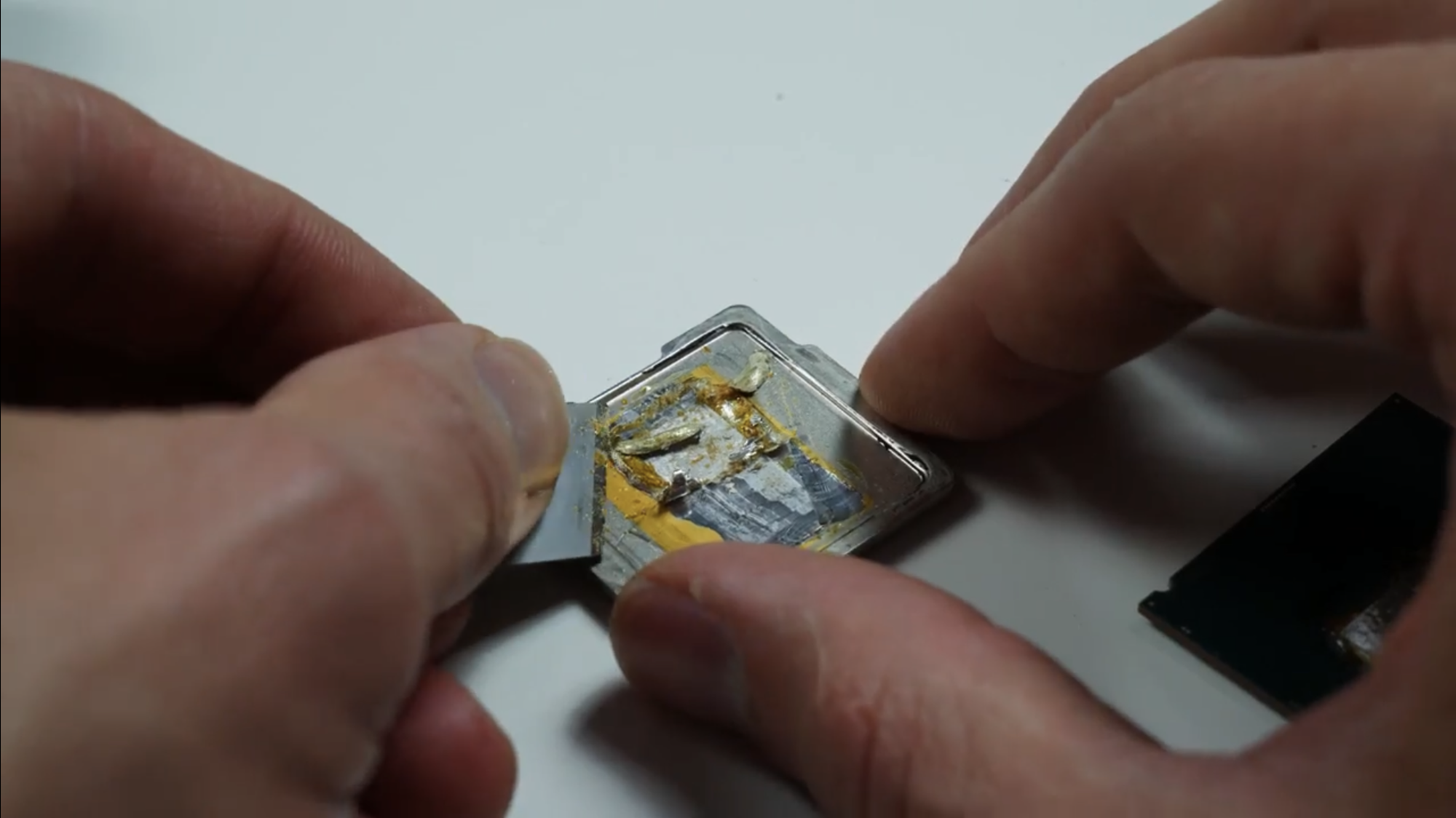
Der8auer noticed that his 9900k was running hotter than it should, especially when compared to an 8700k with inferior TIM. While the extra two cores definitely account for some of the heat, der8auer delidded a 9900k and took some measurements. As it turns out, the 9900k's die is significantly taller than the 8700k. As the CPU sits at the bottom of the silicon "stack", there's more material for that heat to go through. Sanding some of that material off resulted in a significant temperature decrease under load.

Be sure to check out the full video here.
 
I'll watch the video over lunch, but damn sanding a cpu die would scare the crap out of me. So now we need delidding kits, and sanding jigs that ensure we don't sand too far? Wonder if silicon lottery will start selling pre-sanded cpus?
 
Intel isn't going to waste silicone or engineering hours on something you don't need. The 9900K gets hot as hell under the lid, especially overclocked, as the reviews show. Perhaps the material is needed to limit the damage to the CPU over time.

I'll be very interested to see how many people are going to have CPUs getting flaky on them after a year or so of running 5GHz allcore.
 
WOW.

Fascinating info here. Hopefully the X299 Basin Falls refresh doesn't suffer like the 9900K does from a thicker die.
 
LOL, so now de-lidding isnt even enough? You have to SAND your CPU to get the performance you should get OUT OF THE BOX??? Wow....there are no words...
Sanding the cpu isn't a new thing....we called it lapping.

HOWEVER, I doubt I'd do it on such an expensive cpu. I'd rather it be right out of the box, or be cheaper so it doens't kill me to replace it if I screw up.
 
Sanding the cpu isn't a new thing....we called it lapping.

HOWEVER, I doubt I'd do it on such an expensive cpu. I'd rather it be right out of the box, or be cheaper so it doens't kill me to replace it if I screw up.
I remember lapping cpu heat spreaders (last one for me was my Q6600) but I didn't think lapping the cpu die itself was popular.
 
Look, it's not the best solder but it's better than what they were doing.

Are they still only doing it on their top line of processors?
 
Nobody is talking about the solder. The covering over the CPU itself was made thicker, so it's retaining more heat before it even makes it to the solder,

One step forward, four steps back.

This is what happens when I skip through most of the video.

Now I have to watch it properly.
 
Watched the whole video, that was really interesting. I think the most important takeaway here is that yes, delidding still provides a significant benefit even though it was soldered, and Intel made the silicon of the cpu die thicker than the 8700k for some reason. Thinning that silicon layer down further improves temperatures as silicon's thermal conductivity isn't the greatest. I think we'll absolutely see delidded cpus up for sale (he even mentions of course that case king is selling them) but I'm not sure they will offer sanded down cpu dies. It does provide another 5c from delidding alone, but the risk here is so much greater.
 
Nobody is talking about the solder. The covering over the CPU itself was made thicker, so it's retaining more heat before it even makes it to the solder,

One step forward, four steps back.
Without having watched the video, yet, the comments are suggesting this is the area underneath the solder as the actual die is being sanded. We used to lap dies back when they were bare. People did sometimes lap too much but the more likely problem was chipping it when the cooler went on or came off.
 
Holy crap. At this part I would have slipped and put the blade halfway into my thumb.

6F5AEAF2-81D2-4793-BBFD-27EEF9DFFACC.png
 
Without having watched the video, yet, the comments are suggesting this is the area underneath the solder as the actual die is being sanded. We used to lap dies back when they were bare. People did sometimes lap too much but the more likely problem was chipping it when the cooler went on or came off.
Indeed it is the cpu die itself that he sanded. He insists that the circuits are on the bottom of the silicon, so taking some off the top won't kill it.
 
I wonder what the reason was for increasing the die thickness. I doubt it was just arbitrary.
Maybe they needed space for hardware support for Spectre & Meltdown's successors. Or maybe they want to misuse the awesome potential of the 3DXPoint tech AGAIN (Micron, RUN from them and make this into absurdly fast storage PLEASE), by putting it on the new 9000 series for no reason.

Just kidding.... But it's fun to kick sand at Intel and Ngreedia, both companies have proven to me time and time again they don't give a flying fuck about the end user. Intel cares about DELL, Lenovo, etc (bulk sales). And if you pre-ordered anything from Intel or NVIDIA, you get what you deserve. Intel should rename it the 9900k FX.
 
Good video - Dammit, was going to take the plunge with the 9900K, but was really hoping that STIM combined with lots of heavy duty watercooling would really let me push this sucker hard and let it fly. Seems that is not the case here.

While the extra cores the 9900K offers are nice, it appears that Intel is just recycling their current fab tech by increasing the sandwich/packaging thickness and using STIM so that they can not only push it to its limits but also have it hold up to the heavier/beefier heatsinks that will be required in order to cool this monster. I.E. They are already running the clocks much harder/closer to the ragged edge with the 9900K in order to squeeze out every last bit of performance they can from the die to compete/stay out on top against AMD.

The fact that OCing these puppies (even with a great water cooling setup) is only going to take you from 4.9/5 Ghz up to around 5.2Ghz is pretty much damning in that it really demonstrates just how hard Intel is already pushing this silicon. Yes, its a great performer, but there just doesn't seem to be much here as to leeway or options for enthusiasts to exploit in pushing it any further. Having to de-lid and then lap the silicon itself just to eek out another what .1 or .2 Ghz at best? Ah, no thanks, just not worth the time, trouble or risk. Guess I am going to hold out just a bit longer now and see what comes down the pike after the 9900K before upgrading. My 4970K at 4.8Ghz is having a very good 3+ year run it seems... I very much want to upgrade, but I also really want to utilize my water loop to its fullest and would rather invest/upgrade into something that not only offers a massive performance upgrade out of the box, but also offers some headroom that my loop could exploit further. Seems the 9900K is already pushed pretty much to its limits out of the box by Intel and that there's not all that much more that can be exploited further here.
 
Indeed it is the cpu die itself that he sanded. He insists that the circuits are on the bottom of the silicon, so taking some off the top won't kill it.
This is an old technique we used around 20 years ago back when chips came with bare dies. Back then, though, our processors didn't shift through power states but once they were able to lower power demands on the fly lapping the die became much less important. The rule of thumb back then was to not lap past the etching/writing on the die.

The tolerances were a lot less stricter back then, though. Or at least that's what we tended to conclude. There was debate back then whether the convex/concave shape of dies and coolers was intentional or not--but anyone lapping their stuff was trying to make them flat as possible.

Anyway, there are concerns about the height of the chip under the current de-lidding practices. Many people have noticed that once they remove the IHS adhesive it sits slightly lower in the socket resulting in less than ideal compression between the IHS and cooler. This stock height difference makes me wonder if Intel was addressing that concern. There has been speculation that Intel anticipates end-users to de-lid and engineers around that expectation. That reasoning for that speculation is to base it on the belief that Intel expects certain customers to do this to their chips but doesn't want to warranty them (which seems fair to me).
 
My first thought is the thicker silicone was to prevent damage from the solder-IHS process. As dies shrink I gotta believe that the circuit itself becomes more fragile internally especially to heat.
 
The fact that OCing these puppies (even with a great water cooling setup) is only going to take you from 4.9/5 Ghz up to around 5.2Ghz is pretty much damning in that it really demonstrates just how hard Intel is already pushing this silicon. Yes, its a great performer, but there just doesn't seem to be much here as to leeway or options for enthusiasts to exploit in pushing it any further. Having to de-lid and then lap the silicon itself just to eek out another what .1 or .2 Ghz at best? Ah, no thanks, just not worth the time, trouble or risk. Guess I am going to hold out just a bit longer now and see what comes down the pike after the 9900K before upgrading. My 4970K at 4.8Ghz is having a very good 3+ year run it seems... I very much want to upgrade, but I also really want to utilize my water loop to its fullest and would rather invest/upgrade into something that not only offers a massive performance upgrade out of the box, but also offers some headroom that my loop could exploit further. Seems the 9900K is already pushed pretty much to its limits out of the box by Intel and that there's not all that much more that can be exploited further here.
There won't ever be a chip that can be stretched like the chips of yesterday. Every iteration of manufacturing process gets better and more efficient in losses/waste/mistakes/binning. The reason we could overclock an old chip to the same level of the best, most expensive chip is because they were literally the same chip...sometimes you could even see where the manufacturer cut the chip to make it perform at a lower spec (and the fix was to literally draw the connection back and see if the truncated section was capable of working, for example).

Now they've got their manufacturing processes so well-tuned that they can get them down to much better tolerances so you see in the market space processors at 200mhz increments for $20 dollars each step. Things will only get even more efficient with better tolerances so if anything we can expect to see 5mhz increments for dollar differences until customers end up with SKU fatigue and Intel/AMD scales back the offerings.
 
My first thought is the thicker silicone was to prevent damage from the solder-IHS process. As dies shrink I gotta believe that the circuit itself becomes more fragile internally especially to heat.

Agreed - odds are the thicker silicon not only serves to help protect against expansion/compression forces from all the thermal cycling the 9900K cores are going to produce in the larger die due to their running pretty hot from being pushed so hard, but it will also help when it comes to standing up physically to the heavier heatsinks that are going to be hanging off this sucker.
 
My first thought is the thicker silicone was to prevent damage from the solder-IHS process. As dies shrink I gotta believe that the circuit itself becomes more fragile internally especially to heat.
That seems like a viable explanation, too. I don't think this iteration had a die shrink, though.
 
Maybe they needed space for hardware support for Spectre & Meltdown's successors. Or maybe they want to misuse the awesome potential of the 3DXPoint tech AGAIN (Micron, RUN from them and make this into absurdly fast storage PLEASE), by putting it on the new 9000 series for no reason.

Just kidding.... But it's fun to kick sand at Intel and Ngreedia, both companies have proven to me time and time again they don't give a flying fuck about the end user. Intel cares about DELL, Lenovo, etc (bulk sales). And if you pre-ordered anything from Intel or NVIDIA, you get what you deserve. Intel should rename it the 9900k FX.


Hahahaha ... I'm dying .... "Maybe they needed space for hardware support for Spectre & Meltdown's successors" The funniest shit ever right there
 
I mean, I'm OK with delidding an IHS .... I've done this a few times already ... but lapping your CPU die? FUCK NO ......... I'm a diabetic with a slight amount of neuropathy in my hands ( numbness ) and instead of doing a figure 8 I would end up doing a fucked up figure 3 giving my cpu die a slight lean on one of edges ... yeah ... no.
 
Last edited:
There won't ever be a chip that can be stretched like the chips of yesterday. Every iteration of manufacturing process gets better and more efficient in losses/waste/mistakes/binning. The reason we could overclock an old chip to the same level of the best, most expensive chip is because they were literally the same chip...sometimes you could even see where the manufacturer cut the chip to make it perform at a lower spec (and the fix was to literally draw the connection back and see if the truncated section was capable of working, for example).

Now they've got their manufacturing processes so well-tuned that they can get them down to much better tolerances so you see in the market space processors at 200mhz increments for $20 dollars each step. Things will only get even more efficient with better tolerances so if anything we can expect to see 5mhz increments for dollar differences until customers end up with SKU fatigue and Intel/AMD scales back the offerings.

True, an unfortunate consequence of the manufacturing tech getting better and better is that it does close the gap on the tolerances in play so that there's much less left there to play with and exploit by the performance enthusiast crowd. Would have really been nice if the thermal engineering and the new STIM that the 9900K sports could have been better designed to be exploited via superior cooling such as a good water loop though. Having to still de-lid and lap the silicon on the 9900K just to get the thermal transfer performance up to snuff really blows. :-(

I'm thinking I may just sit this out a bit longer and wait for 10nm.
 
Nothing too scary about lapping cpu, esp when we had no IHS cpu dies as common place back in the day where you'd chip the die when trying not to put a screw driver though your motherboard because the cpu retention mechanism was super suspect
 
  • Like
Reactions: Jza
like this
Nothing too scary about lapping cpu, esp when we had no IHS cpu dies as common place back in the day where you'd chip the die when trying not to put a screw driver though your motherboard because the cpu retention mechanism was super suspect
Ah the good ol' days of aiming a flat head screw driver with 100 pounds of pressure behind it at your socket A mainboard as you try to get the retention spring around that white tab. The days of crunching the corner of your CPU die and still using it just fine after rocking your all copper heatsink just a little too much during install. With wonderful 60mm fans spinning sometimes at speeds in excess of 5000 rpm. I've never sanded a CPU die, but I did sand the hell out of a Geforce 3 Ti once. Thanks for the memories.
 
I lapped the IHS and heatsink on a Q9550 with a piece of glass up to 2000 grit. Thought that was pretty extreme at the time. Potentially compromising the die is nutzo.
 
Back
Top