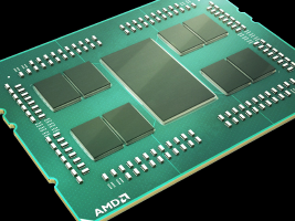
Chiplet Based Designs are Gaining Momentum

AlphaAtlas

[H]ard|Gawd
Staff member
Joined
Mar 3, 2018
Messages
1,713
While AMD recently gained notoriety for using a "chiplet" based design in their EPYC CPUs, Semiconductor Engineering says that numerous other companies are working on chiplet-based products. The report claims that Marvell is actually the first, and only, company to deploy the chiplet concept commercially so far, but a senior director at the company said "Next year you’ll be hearing a lot more about chiplets." Multiple industry leaders claim that the chiplet approach is becoming more viable as Moore's Law "comes to a grinding halt." Nevertheless, there are still some major hurdles to overcome with multi-chip designs, like added testing complexities, packaging concerns, and managing IPs from different vendors, among many others. But Semi Engineering's experts seem to think chiplets are the next logical step in silicon chip design, and their opinions are worth a read.

"Chiplets will increase the rate of sales, and there will be more innovation" said Amin Shokrollahi, CEO of Kandou Bus. "And this will accelerate innovation because you are designing only one part. This has been the driver among IP houses and the IP business in general. You grab one IP from here and another from there. But where this has run into problems is putting these IPs together. That part is tough.
 
Multiple industry leaders claim that the chiplet approach is becoming more viable as Moore's Law "comes to a grinding halt.
I've been saying a paradigm shift was going to be needed to move beyond the physical limitations of where we are with CPUs at this point.
Didn't think it would end up being chiplets, though! o_O
 
I've been saying a paradigm shift was going to be needed to move beyond the physical limitations of where we are with CPUs at this point.
Didn't think it would end up being chiplets, though! o_O

Well, the industry is taking multiple approaches. But chiplets seem to be something we'll see more of in 2-4 years, as opposed to other tech that will take longer to commercialize.
 
so what exactly are the advantages that allow better performance/less power/etc?
 
so what exactly are the advantages that allow better performance/less power/etc?
You're not making a monolithic die that contains everything. The chiplets spread out heat generation over a larger surface area. Plus, in terms of price, chiplets are much smaller, reducing the cost in manufacturing because monolithic dies will have more defects per part. If a few chiplets are bad, that's less than the cost of a monolithic die.
 
The chiplet design doesn't have anything to do with / or to mitigate the Spectre / Meltdown hardware flaws does it?
 
The chiplet design doesn't have anything to do with / or to mitigate the Spectre / Meltdown hardware flaws does it?
No. However, strictly speaking, you can now make processors with more physical cores, and don't really need SMT (Hyper-Threading) as much to get good performance. Not having SMT mitigates a large number of attack vectors.
 
Nevertheless, there are still some major hurdles to overcome with multi-chip designs, like added testing complexities, packaging concerns, and managing IPs from different vendors, among many others. But Semi Engineering's experts seem to think chiplets are the next logical step in silicon chip design, and their opinions are worth a read.

"Chiplets will increase the rate of sales, and there will be more innovation" said Amin Shokrollahi, CEO of Kandou Bus. "And this will accelerate innovation because you are designing only one part. This has been the driver among IP houses and the IP business in general. You grab one IP from here and another from there. But where this has run into problems is putting these IPs together. That part is tough.
Strange...how is this different than using a Via southbridge or an asmedia usb controller? I would think validation, testing, etc. would be the same regardless of where the chip is...
 
Strange...how is this different than using a Via southbridge or an asmedia usb controller? I would think validation, testing, etc. would be the same regardless of where the chip is...
It is different in that the chiplets share very crucial parts, like cache memory, I/O hardware, memory controller. There's also the fact that those chiplets do still all live 'in the same house' as in, package. Pin configuration isn't changing too much when you stay on the same socket (AM4 for AMD) so you've got to validate that the package can deliver properly for all the chiplets inside of it. Then you've got the intra-chip testing; when you have 4 vs 8 chiplets for instance, the internal pathways are very different: longer traces, more resistance, higher voltages etc.

When you are looking at say an Asmedia USB, that chip has to adhere to a defined protocol that is the same as other devices in the system. It's not as closely tied to other components as a chiplet would be. That's where industry standards take a lot of the guesswork out and put validation on each vendor who wants to provide parts.
 
This is more of a manufacturing breakthrough than a sheer performance shift, though one ALWAYS affects the other.

Chiplets are MUCH more efficient to produce. If a single 500mm^2 die has a chip-killing defect, that's 500mm^2 of useless silicon. With Chiplets that defect might only effect 120mm^2 of silicon, and is much cheaper to mitigate, making the binning process produce high-performing SKUs much more frequently.
 
Strange...how is this different than using a Via southbridge or an asmedia usb controller? I would think validation, testing, etc. would be the same regardless of where the chip is...

It isn't. And anyone who says it is doesn't understand chip design or validation.
 
It is different in that the chiplets share very crucial parts, like cache memory, I/O hardware, memory controller. There's also the fact that those chiplets do still all live 'in the same house' as in, package. Pin configuration isn't changing too much when you stay on the same socket (AM4 for AMD) so you've got to validate that the package can deliver properly for all the chiplets inside of it. Then you've got the intra-chip testing; when you have 4 vs 8 chiplets for instance, the internal pathways are very different: longer traces, more resistance, higher voltages etc.

When you are looking at say an Asmedia USB, that chip has to adhere to a defined protocol that is the same as other devices in the system. It's not as closely tied to other components as a chiplet would be. That's where industry standards take a lot of the guesswork out and put validation on each vendor who wants to provide parts.
The big deal with this is the reduction in production costs due to higher yealds. The down side is that it adds more complexity to the package production and increases intra-CPU latency. It will be interesting to see how thermals are impacted by this and how the change in thermal performance actually affects processing performance.
 
so what exactly are the advantages that allow better performance/less power/etc?

Instead of making one die with 8 cores thata can go
2.0ghz
5.0ghz
5.0ghz
5.0ghz
5.0ghz
5.0ghz
5.0ghz
5.0ghz
and have to sell it as a 2ghz unit

You are isntead making small dies of 1 core each and combined them together
2.0ghz ( will be repalced with a 5ghz chiplets from some where else)
5.0ghz
5.0ghz
5.0ghz
5.0ghz
5.0ghz
5.0ghz
5.0ghz
Sells at a 5ghz unity


or to put it in another word: the chains is not longer as weak as the weakest chink

more info:
 
You hear that Mr. Anderson..? That is the sound of inevitability. It is the sound of chiplets being fabricated.

chiplets-1.png


Neo: Mmmm, my favorite!

...

Agent Smith: Nooo you foolish meatbag, this!

chiplets-2.png


Neo: Whoah! Dude...
 
I hope we see some sort of a chiplet GPU where the system sees it as one GPU..... Might give AMD an advantage and provide us with more high end competition / lower prices.
 
why's that?

I assume he is referring to latency issues (which is the only thing I can think of) but what many forget is that very large monolithic dies have their own latency issues as well. It is going to be interesting to see how Zen2 plays out since AMD doubled down on that lovely L3 cache, at least for server SKUs. That, combined with the front/back end changes should make it very interesting vs Zen+ and especially Zen.
 
why's that?

A monolithic chip is much simpler design wise and will have much better baseline performance. As you disaggregate, you have to design an entire communication network, increase latency, reduce bandwidth, add chip to chip physical communication circuits, and expend more power on communication (on chip pj/bit/s is orders of magnitude better than interposer/intra-package which is orders of magnitude better than extra-package). The reason to go chiplet is yield, yield, yield, yield.
 
The chiplet thing is being looked at by pretty much everyone involved at the high end. AMD is the first to market with a CPU but Intel has been shipping a FPGA for a while that uses EMIB bridges for its transceivers (which don't scale as nicely as logic on new fab processes) + HBM2. nVidia has a research paper detailing some there internal efforts and it is widely speculated even before there Epyc announcement that AMD would be doing this for GPUs too. Intel on the CPU side has their Sky Lake-X cores with a grid based topology which should easily scale up to a chiplet implementation.

Only high end player that I haven't seen chiplet news from is a company that kinda does it already: IBM. They do a lot MCM work in the big iron server and mainframe space that going the chiplet route wouldn't even be that news worthy.
 
Back
Top