AMD Polaris 10 Has 390/390X Performance

if it is indeed running at 1.3 with samples I bet its gonna be one hell of a performer for the price. We shall see..

That test sample on SiSoft is 5.83 TFLOPS which puts it close to the 390X at 5.91 TFLOPS assuming no architecture changes. It's putting it much more in line with the original rumor of 390X performance at $200 that somehow warped to 390X performance at $300 when it was combined with the rumor that said 980Ti performance at $300. Of course all those rumors are probably wrong.
 
Last edited:
That test sample on SiSoft is 5.83 TFLOPS which puts it close to the 390X at 5.91 TFLOPS assuming no architecture changes. It's putting it much more in line with the original rumor of 390X performance at $200 that somehow warped to 390X performance at $300 when it was combined with the rumor that said 980Ti performance at $300. Of course all those rumors are probably wrong.

True, they are taking in to account just clock speed jump with less shaders. But we do know for a fact they have changed pretty much the whole front end to improve ipc. If we are getting atleast 20% performance there than it could creep up to 980ti or 1070. Ofcourse its all speculation but its seems viable that they have made some architecture improvements. we shall see.
 
Front end improvements give around ~18% perf/watt, don't expect all of that to go to performance.... I would say around 10% to performance and 8% to wattage reduction.

30/70 split from architecture and node respectively, to give a 2.5x perf/watt advantage over today's high end chips (r390x)

Now if we go by 2.0 perf per watt from Tonga, that will be even less....

They actually gave us all the numbers to figure out what the performance will be for a set wattage.

If they are at ~100 watts, they will get Tonga performance, if they are at ~120 watts they get 390 to 390x performance, if they are at ~150 watts 390x performance Fury X performance.
 
Last edited:
True, they are taking in to account just clock speed jump with less shaders. But we do know for a fact they have changed pretty much the whole front end to improve ipc. If we are getting atleast 20% performance there than it could creep up to 980ti or 1070. Ofcourse its all speculation but its seems viable that they have made some architecture improvements. we shall see.

The cutdown Polaris 10 could be incredibly close to the 1070 if it has the clockspeeds to compete. The 1070 being cutdown by 25% is effectively a 234mm² die. If the Polaris 10 is cutdown 10%, that would be 209mm², or 225mm² when you formulate the transistor density of 14nm compared to 16nm. That also puts the full Polaris 10 which is 232mm² effectively above the 1070 with 250mm² equivalent die space.
 
Last edited:
you can't compare that way, as each architecture is different, core counts mean jack, just like Tflops...... don't use those as metrics as one doesn't equal, its like saying Fiji should blow away the 980ti at stock clocks, it just doesn't happen.

Also who gives a crap about die size and how does that affect performance of two vastly different architectures?
 
Here
Front end improvements give around ~18% perf/watt, don't expect all of that to go to performance.... I would say around 10% to performance and 8% to wattage reduction.

30/70 split from architecture and node respectively, to give a 2.5x perf/watt advantage over today's high end chips (r390x)

Now if we go by 2.0 perf per watt from Tonga, that will be even less....

They actually gave us all the numbers to figure out what the performance will be for a set wattage.

If they are at ~100 watts, they will get Tonga performance, if they are at ~120 watts they get 390 to 390x performance, if they are at ~150 watts 390x performance Fury X performance.

Here's hoping that even if it's 120w you'll still be able to overclock up to Fury X levels.
 
you can't compare that way, as each architecture is different, core counts mean jack, just like Tflops...... don't use those as metrics as one doesn't equal, its like saying Fiji should blow away the 980ti at stock clocks, it just doesn't happen.

Considering we hardly have any concrete information on GCN4, we can only compare with what we know.

If we were to try and compare Fiji and Maxwell by die size, we would need to first deduct the memory controllers from the die sizes of the FuryX and 980Ti.
 
Die-size is not a concrete way to go about estimating wholy different architectures, however its a good way to compare like-for-like.

However, we do know that GCN in general hasn't received a huge boost in performance per core. Usually GCN improvements are done through adding features and reducing power usage. clock-for-clock, core-for-core I don't think GCN 1.0 is any slower than GCN 3.0
 
If AMD promise of 2.5x perf/w is true for Polaris over a 390x, here is the math

So if the top Polaris is a 175w chip x 2.5 x 390xPerf/250w = 1.75 times the performance of a 390x
150w x 2.5 x 1/250w = 1.5 times the performance of a 390x
130w x 2.5 x 1/250w = 1.3 times the performance of a 390x

If 390x is using full spec for pcie connectors and motherboard = 300w (390x unless doing furmark is less than 300w at stock clocks)

Polaris at 175w x 2.5 x 1/300 = 1.46 times the performance of a 390x
150w x 2.5 x 1/300 = 1.25 times the performance of a 390x
130w x 2.5 x 1/300 = 1.08 times the performance of a 390x

Now when AMD put out the Nano perf/w over the 290x in the past - it was right on the money.

So the top end Polaris should be faster than a 390x. Since we are dealing with multiple skews, unlike the Nano which was just one, the 2.5x perf/w maybe just relevant to the lowest model. I would not think so since the Perf/w is comparing it to the 390x which to me means comparing it to the 490x.
 
Die-size is not a concrete way to go about estimating wholy different architectures, however its a good way to compare like-for-like.

However, we do know that GCN in general hasn't received a huge boost in performance per core. Usually GCN improvements are done through adding features and reducing power usage. clock-for-clock, core-for-core I don't think GCN 1.0 is any slower than GCN 3.0

You don't have to improve the performance of the actual Stream processors generation to generation (assuming that is what you mean).

Here is an example, you can have better die size efficiency (and in other areas) via color compression instead of investing more transistors (and therefore die space) in your memory controllers. Tonga for instance does this, well kind of since they still devoted transistors to having enough controllers for a 384 bit bus that is just never enabled. Maybe a better example would that Nvidia did this with Kepler->Maxwell->Pascal.
 
If AMD promise of 2.5x perf/w is true for Polaris over a 390x, here is the math
So if the top Polaris is a 175w chip x 2.5 x 390xPerf/250w = 1.75 times the performance of a 390x
150w x 2.5 x 1/250w = 1.5 times the performance of a 390x
130w x 2.5 x 1/250w = 1.3 times the performance of a 390x
If 390x is using full spec for pcie connectors and motherboard = 300w (390x unless doing furmark is less than 300w at stock clocks)
Polaris at 175w x 2.5 x 1/300 = 1.46 times the performance of a 390x
150w x 2.5 x 1/300 = 1.25 times the performance of a 390x
130w x 2.5 x 1/300 = 1.08 times the performance of a 390x
Now when AMD put out the Nano perf/w over the 290x in the past - it was right on the money.
So the top end Polaris should be faster than a 390x. Since we are dealing with multiple skews, unlike the Nano which was just one, the 2.5x perf/w maybe just relevant to the lowest model. I would not think so since the Perf/w is comparing it to the 390x which to me means comparing it to the 490x.

It depends on how the 2.5 figure was calculated was it just the chip or the whole board ? If it was the whole board what ram was used for any of it DDR5 HBM?
 
If AMD promise of 2.5x perf/w is true for Polaris over a 390x, here is the math

So if the top Polaris is a 175w chip x 2.5 x 390xPerf/250w = 1.75 times the performance of a 390x
150w x 2.5 x 1/250w = 1.5 times the performance of a 390x
130w x 2.5 x 1/250w = 1.3 times the performance of a 390x

If 390x is using full spec for pcie connectors and motherboard = 300w (390x unless doing furmark is less than 300w at stock clocks)

Polaris at 175w x 2.5 x 1/300 = 1.46 times the performance of a 390x
150w x 2.5 x 1/300 = 1.25 times the performance of a 390x
130w x 2.5 x 1/300 = 1.08 times the performance of a 390x

Now when AMD put out the Nano perf/w over the 290x in the past - it was right on the money.

So the top end Polaris should be faster than a 390x. Since we are dealing with multiple skews, unlike the Nano which was just one, the 2.5x perf/w maybe just relevant to the lowest model. I would not think so since the Perf/w is comparing it to the 390x which to me means comparing it to the 490x.

Doesn't go up 2.5 times the perf/watt, is always counted from the down. Take the perf/wattage of the 390x and calculate from there. And when was the 390x 250 watts? Its rated at 275 watts and uses over 300 watts many times and that is the card alone.

But yeah easy to calculate because AMD gave use best case numbers. There is nothing to really speculate about performance, we just don't know what wattage Polaris will come at, that is it.
 
Last edited:
Considering we hardly have any concrete information on GCN4, we can only compare with what we know.

If we were to try and compare Fiji and Maxwell by die size, we would need to first deduct the memory controllers from the die sizes of the FuryX and 980Ti.


How many times have we seen die size and alu counts mean nothing, how many generations?

And fury X has its memory controller is not on the GPU.
 
Last edited:
The removal we are seeing of a major portion of the HAL (Hardware Abstraction Layer) with Vulkan and DX12, but present in DX11 and under should help considerably in optimizing the GPU resources which were in good portion wasted and contributed to the reason why sometimes die size, on the same node, didn't equate to performance.
 
PS if we don't want to quarrel over what current chip AMD is basing this off of, just use Tonga (r380) and 2.0 perf/watt increase because that is what the CFO and CEO stated in their latest financial conference call and its their best perf/watt chip out there. TBP, typical board power is what AMD uses to give an idea of what their boards use and its at 190 watts.

So 95 watts will give ya Tonga performance, and as you increase frequency (wattage) you might not get a linear scale, but its pretty easy to figure out what the best case is if you do.

Pretty dicey assumption since FinFET gets twitchy and hot as soon as you start ramping voltages unlike previous gens.
 
Pretty dicey assumption since FinFET gets twitchy and hot as soon as you start ramping voltages unlike previous gens.


Its not dicey, AMD used their CURRENT cards to get their perf/watt numbers, they didn't make them out of thin air. Going by THEIR numbers you will end up with what they got.

The only time those numbers will go out of wack is if there were leakage issues that would skew the numbers, so if you presume there is leakage issues with Tonga, if that was the case, that 2.0 perf/watt would actually be less than what was stated because Finfet won't come across that issue, since voltage should be lower at the wattage needed.

Which would you prefer, less that 2.0 or 2.0? I'm taking it as 2.0 since this is best case.

If we extrapolate a 150 watt Polaris card, what would the performance be? 55% increase in power, if we have a perfect linear scaling of frequency we get 55% increase in frequency, if we have a perfect scaling of performance that is a 55% increase in performance, we end up with ~between Fury X 980ti performance based on resolution, but most likely we won't get perfectly linear increases.......
 
Last edited:
No its not its on the bottom of the memory stack.

960px-High_Bandwidth_Memory_schematic.svg.png


This is why third party companies can make memory controllers for HBM.

This is from AMD Fiji presentation

05-interposerstacked.jpg


The logic die is the memory controller. This was the reason why AMD didn't have the ability to overclock the memory when launched too.

Did you miss the memory controller on the top left of the top picture, on the GPU next to the display controller?
 
do yo see that in AMD's diagram?

The second diagram is AMD's diagram.....

It can be done either way, but AMD didn't incorporate the memory controller into the GPU die, its pointless to do so because it just wastes space which they could use for other parts of the GPU.
 
do yo see that in AMD's diagram?

The second diagram is AMD's diagram.....

It can be done either way, but AMD didn't incorporate the memory controller into the GPU die, its pointless to do so because it just wastes space which they could use for other parts of the GPU.


Yes, they did.

HBM does require a new memory controller as compared to what was utilized with GDDR5. There are 8 new memory controllers on Fiji that interface directly with the HBM modules. These are supposedly more simple than what we have seen with GDDR5 due to not having to work at high frequencies. There is also the logic chips at the base of the stacked modules and the less exotic interface needed to address those units as again compared to GDDR5. The changes have resulted in higher bandwidth, lower latency, and lower power consumption as compared to previous units. It also likely means a smaller amount of die space needed for these units.

AMD Exposes Fiji to the World: HBM for the Enthusiast | The Fiji GPU
 
Everything in white is not part of the die. Unless you want to put the PCI 3.0 express bus part of the die too ;)
Even if they had some portion of the mc's on die its much smaller, so lets take that into consideration then?

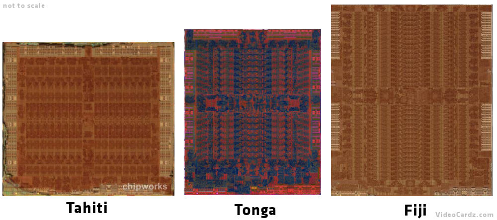
Tahiti-vs-Tonga-vs-Fiji-dieshots.jpg


There is a die shot, you want to tell me the memory controllers take up 60mm2 in Fiji's die shot????
 
Last edited:
Everything in white is not part of the die. Unless you want to put the PCI 3.0 express bus part of the die too ;)
Even if they had some portion of the mc's on die its much smaller, so lets take that into consideration then?

Are you still digging in your heels?

With HBM in Fiji, it is a lot simpler even though it is wider and has a net higher bandwidth. Now only about 10% of the die is the HBM controller, roughly 60mm^2, even though bandwidth goes up significantly saving both power and obviously expensive silicon.

AMD talks Fiji, Fiji X, and a few odd bits of tech - SemiAccurate
 
dude its semi accurate Charlie is retard LOL!, I just posted a pic of FIji's die, do the math yourself.

if I got the pixel amounts right its ~40mm. Don't have photoshop on my system so can't do an accurate amount, eyeballing it with paint. Then compare it to tonga and see the difference in amount of die space needed for each.
 
Last edited:
dude its semi accurate Charlie is retard LOL!, I just posted a pic of FIji's die, do the math yourself.

if I got the pixel amounts right its ~40mm. Don't have photoshop on my system so can't do an accurate amount, eyeballing it with paint. Then compare it to tonga and see the difference in amount of die space needed for each.

So wait, now you are admitting there's a memory controller on die?
 
Seems that way part of it in on the die. Any case you still have to factor in less die space around 50% less and less clocks for that specific part of the die in the neighborhood of 4 times less.

And it doesn't matter of all this talk because AMD already gave us best case numbers for perf/watt, that is the easiest thing to go by to get what the possible performance of Polaris can be based on a set base wattage.

The only way I can see Polaris even getting close to a 1070 is if they hit ~200 watts, if rumors of the 1070 being around a Titan X is true. And that is if you have prefect scaling of wattage to frequency to actual performance. We still haven't even factored in what the memory is clocked at either that might make a difference as well albeit small.
 
Last edited:
There's a few bits of information learned from the AMD Polaris meeting today.

CataclysmZA said:
There were very, very few new details announced. However, there were some new bits:

  • AMD's options with FinFET are to target higher clock speeds at the same relative power to an older gen card, or lower power with comparable performance.
  • GDDR5X is definitely supported on Polaris, at least with Polaris 10.
  • There are new VR features in the works. Nothing said about them, but possibly a counter to NVIDIA's stuff.
  • FreeSync 4K 120Hz monitors with LFC are just around the corner.
  • FreeSync and HDR is currently not an option now.
  • You can pass through sound effects generated by TrueAudio into your streams and recorded videos now. Previously this was mixed down to stereo only.
  • Game DVR works up to 4K 60Hz with H.265 encode and decode.

[SiSoft] Polaris at almost 1,3GHz - Frequenzy of test samples increasing - Page 13
 
More from that thread:

ebduncan said:
They clearly don't want to give polaris details until official launch day. However, we did learn that AMD didn't target the highest performance possible on finfets, but remained conservative relative to performance per watt. They did mention AIB board partners will likely release products which push the clock speeds.

They also confirmed there will be more than 2 cards based on polaris, though will likely be released at a different time. Which makes me question their naming scheme. We know of polaris 11, and polaris 10. P10 is the performance card, while p11 is the low power card. If they release more cards one would assume they would be higher performing parts, so what would they be called Polaris 9? polaris 12? leads to confusion haha.

ebduncan said:
IE setting the TDP low say 120watts. Instead of say 150 watts to extract more performance with higher clock speeds. Better known as overclocking headroom.

CataclysmZA said:
Basically leaving a sizeable amount of headroom for partners to launch new, faster cards, and to offer different variants of the same cards that aren't just different fans for identical performance.

This was NVIDIA's policy with Maxwell, where Tom Petersen openly stated that they knew the cards could be clocked higher to increase the performance gap and offer more value to consumers, but at the end of the day it's better from an AIB relationship standpoint to let the other brands do that on their own. We've had an amazing run of cards on Maxwell as a result, and lots of different options with their own performance profiles. Just about every card saw much improved performance when overclocked.


This plays into it as well. NVIDIA intentionally showed a 2.1GHz clock on the Pascal reveal to show how capable it is with the Founder's Edition reference cooler at maximum fan speed. But their official performance figures on the Geforce website are much lower than what you're typically going to find in the custom cooler market.
 
So I decided to take the 380X and try to use it to determine the power of the 67DF:C7 simply by extrapolating from a random 3DMark 2013 Firestrike benchmark I found. the 67DF:C7 from here has 12.5% more stream processors and 22% higher clock speed. I multiplied the 380X score of 8,457 by 12.5% and then again by 22%. It places the 3DMark 2013 Firestrike score at 11,607, just below the 390X at 11,686. Those scores are in line with the 5.8 TFLOPS of the 67DF:C7 and the 5.9 TFLOPS of the 390X.

So I then decided to do the same thing for the 67C0 which is speculated to be full Polaris 10 at 2560 stream processors which would be 25% more stream processors than a 380X. If you keep the clockspeed the same, you are at 12,896 which is still well under 15,656 of the 980Ti. To get in range of the 980Ti, it would need to be clocked near 1500 Mhz for a score of 15,721 which beats it. If you take the 67DF:C7 and place it at 1500 Mhz, it comes in at 13,795.

Of course all this is based on the assumption it's only the 380X with more cores and higher clockspeed.

I then decided to see if I could do something similar with the 1080 just to see where it would end up. The 1080 has 25% more CUDA cores and 42.5% higher boost clock speed than the 980 which would place it at 19,893 on Firestrike. I then went and looked to see if they actually had a 3DMark 2013 Firestrike benchmark for it, and yes they did. It's score came in at 19,370, really close to my extrapolation. When I calculate, I use rounded numbers and percentages and it came within a 2.6% margin.

I then decided to use the same process again for the 1070. The 1070 as 6.3% fewer CUDA cores than the 980 and 39% higher clockspeed. This places it at a 14,546 Firestrike score, more than the FuryX, but less than the 980Ti.

380X: 8,457
67DF:C7 (1266 Mhz): 11,607
980: 11,168
390X: 11,686
67C0 (1266 Mhz): 12,896
67DF:C7 (1500 Mhz): 13,795
Fury X: 14,374
1070: 14,546
980 Ti: 15,656
67C0 (1500 Mhz): 15,721
1080: 19,370
1080 (extrapolation): 19,893

Edit: Corrected some mistakes.
 
Last edited:
From someone I know, he been told to expect P10 to be 20% faster compared to 970 card, under DX12, which of course is not that fair knowing that 900 cards dont do well under DX12 and nvidia fixed with their new Pascal.
Remains to be seen if its just BS from my friend sources or the real deal.
 
From someone I know, he been told to expect P10 to be 20% faster compared to 970 card, under DX12, which of course is not that fair knowing that 900 cards dont do well under DX12 and nvidia fixed with their new Pascal.
Remains to be seen if its just BS from my friend sources or the real deal.

AMD's 390/390x/Furies are CURRENTLY in DX12 equal to or considerably outperforming 980Ti as well as everything else nVidia depending on game, so no, this laughable rumor is ALREADY BS, and laughable BS at that.
 
The AMD Webinar Sneak Peak was today, and we've got the details - Tech Altar

AMD didn’t say much about performance but they specified that they were able do get to get more performance out of each transistor not only thanks to 14nm FinFET process but also by virtue of the various optimizations within the Polaris architecture itself.

Now probably the most interesting part of the whole QA session. We asked them if the efficiency improvements that AMD specified in their previous presentations are uniform for all GPUs AMD will offer or if it’s just for the most efficient GPU of the whole family. We were lucky enough to get my question answered with a little tiny bit of extra unexpected spice. AMD answered that there will be wide range of different board designs which means some will have different clocks than others. This means that some will be more efficient than others but generally the capability and improvements will be there.
 
click bait article lol.. we've got the details about nothing lol.
 
Back
Top