AMD patents GPU chiplet designs

Marees

2[H]4U
Joined
Sep 28, 2018
Messages
2,075
new patent submitted to the US Patent Office on December 31 describes the AMD approach to potential GPU chiplet design, by implementing ‘high bandwidth passive crosslinks.

According to the patent, a primary GPU chipset would be direct ‘communicably coupled’ to the CPU, while each of the secondary GPU chiplets in the array would be coupled to the first GPU via a passive crosslink.

In this sense, AMD considered passive crosslink as communication wires between chiplets that are placed on a single interposer. (in multiple layers if needed).

In conventional GPU designs, each of the GPU features its own last-level cache (LLC), but in order to avoid problematic synchronization, AMD thinks that each of the GPU chiplets should feature its own LLC, but in a way that each of those caches is ‘communicably coupled’ to physical resources so that the cache remains ‘unified and remains coherent across all GPU chiplets’.

Source: Freepatents via @davideneco25320

https://videocardz.com/newz/amd-pat...4pNlj-nJKIRA64fjWs-jfxliMIF3RN8XGZ7JsBYtG9WnQ
 
Uhh...this is tech beyond my understanding.

Does this mean I can find an AMD video card soon? ;)
I'm thinking this means Crossfire without the lag. See 3Dfx Voodoo 5-6000 for reference.

Looks like they're leveraging their CPU multi-core design to improve their GPU designs? ATI acquisition finally paying off?
 
Uhh...this is tech beyond my understanding.

Does this mean I can find an AMD video card soon? ;)
I’m having a hard time understanding it as well but it looks like a better method for placing a GPU on the CPU package but not having contained inside the CPU die. It appears similar of an Intel patent for their new Xe chips
 
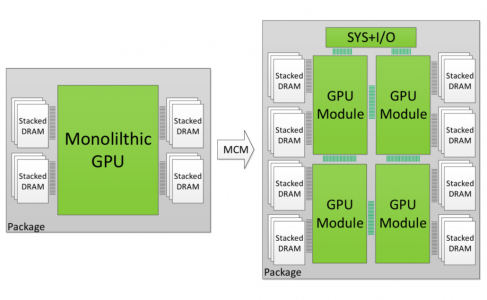
-GPU-Launching-in-2018-Could-Be-MCM-Based-1030x635.png

"theoretically speaking, it should work better in all regards for GPUs which are parallel devices than for CPUs which are serial devices. Not only that but you are looking at massive yield gains from just shifting to an MCM based approach instead of a monolithic die."
 
Last edited:
Ah...Ryzen for GPU? Meaning, Chiplets scattered about on the PCB? Much more yield per wafer and thereby lower prices, AND higher performance?

Hoping the 7000 series come out soon. ;)
I’m far more interested in seeing how they manage to present the package to the OS as a single cohesive GPU. This doesn’t look too dissimilar to any other multi GPU configuration so how will it spread the load across the multiple chips? Or is this their implementation plan for when multiGPU code is more prevalent in existing software?
 
This is just a patent. Still we know AMD has moved a lot of their Ryzen engineers over to the Radeon group. So who knows. Perhaps this is coming as early as 7000s. They used a lot of Ryzen ideas this generation.

However yes if the got this working, it would no doubt help a ton with shortages. Same logic as the Ryzen chips... instead of one 600nm size chip you can fab a cheap controller chip, and a bunch of smaller GPU chiplets.

It would be no more SLI like then Ryzen is dual socket like. The OS would be talking to the controller chip not each chiplet. Yes there are latency issues to deal with just like there is for Ryzen chiplets.... however the OS sees one physical CPU not 2.
 
I’m far more interested in seeing how they manage to present the package to the OS as a single cohesive GPU. This doesn’t look too dissimilar to any other multi GPU configuration so how will it spread the load across the multiple chips? Or is this their implementation plan for when multiGPU code is more prevalent in existing software?
I'm sure it'll be just the way it's done now... they have multiple CU's on a single GPU with some method of handing out instructions on what to do for each one. If the CU's are spread on a single die or multiple, it's still the same concept, just slightly more latency, which is probably why they've been pushing the cache architecture in anticipation. It's not to much different than a chiplet CPU with an I/O die (I mean, conceptually, obviously implementation is a bit more difficult). I don't imagine they'll install 4 full GPU's on chiplets without something to coordinate the memory accesses and coordination. I don't think their plan is to go to software, that would be highly inefficient.
 
I'm sure it'll be just the way it's done now... they have multiple CU's on a single GPU with some method of handing out instructions on what to do for each one. If the CU's are spread on a single die or multiple, it's still the same concept, just slightly more latency, which is probably why they've been pushing the cache architecture in anticipation. It's not to much different than a chiplet CPU with an I/O die (I mean, conceptually, obviously implementation is a bit more difficult). I don't imagine they'll install 4 full GPU's on chiplets without something to coordinate the memory accesses and coordination. I don't think their plan is to go to software, that would be highly inefficient.
I agree but their supposed attempts to date at presenting their packages as a uniformed GPU have been bad. NVidia nor Intel have faired much better which is why both NVidia and Intel have been working with developers very closely for the last year to implement multi GPU for Vulkan, and DX12 at a software level. If AMD has made some sort of breakthrough that’s great but if they have their holding that one pretty close.
 
View attachment 315133

"theoretically speaking, it should work better in all regards for GPUs which are parallel devices than for CPUs which are serial devices. Not only that but you are looking at massive yield gains from just shifting to an MCM based approach instead of a monolithic die."
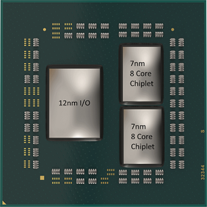
this doesn't seem viable in the long term with those I/O dies being huge and massively wasteful on the substrates


way too big currently:


1609613225486.png
 
I agree but their supposed attempts to date at presenting their packages as a uniformed GPU have been bad. NVidia nor Intel have faired much better which is why both NVidia and Intel have been working with developers very closely for the last year to implement multi GPU for Vulkan, and DX12 at a software level. If AMD has made some sort of breakthrough that’s great but if they have their holding that one pretty close.
The only "supposed attempt" to date is the Ryzen CPU line... and it seems perfectly fine to me. MCM hasn't been done on GPU's, the only thing done on GPU's where literally 2 GPU's slapped onto one circuit board. They weren't really integrated, they were just sharing a single PCB. So, you can't really compare this to previous attempts because it's completely different. How well it works, well, that's obviously something to be seen, and seeing how it took some time for Ryzen to get to the point where the latencies weren't to detrimental, I feel they will need a decent cache system in place to be able to not really kill performance. The current cache system seems to be doing pretty well with such a narrow/slow (comparatively) bus. Right now their 256-bit GDDR6 (512GB/s) is competing against a 320-bit GDDR6X (higher speed, 760GB/s) card and keeping pace pretty well in most situations (at least raster, raytracing is another story but I don't think the cache is to fault here). I think this is going to be critical for the MCM design in order to not completely saturate the interconnect and create to much contention. Will be interesting to see how the implementation goes if they ever follow through down this route. It would be good for yields to be able to make smaller pieces. It also seems similar to how Intel is planning to stitch together their XE line with the ability to put multiple chips on one board to fill multiple markets.
 
The only "supposed attempt" to date is the Ryzen CPU line... and it seems perfectly fine to me. MCM hasn't been done on GPU's, the only thing done on GPU's where literally 2 GPU's slapped onto one circuit board. They weren't really integrated, they were just sharing a single PCB. So, you can't really compare this to previous attempts because it's completely different. How well it works, well, that's obviously something to be seen, and seeing how it took some time for Ryzen to get to the point where the latencies weren't to detrimental, I feel they will need a decent cache system in place to be able to not really kill performance. The current cache system seems to be doing pretty well with such a narrow/slow (comparatively) bus. Right now their 256-bit GDDR6 (512GB/s) is competing against a 320-bit GDDR6X (higher speed, 760GB/s) card and keeping pace pretty well in most situations (at least raster, raytracing is another story but I don't think the cache is to fault here). I think this is going to be critical for the MCM design in order to not completely saturate the interconnect and create to much contention. Will be interesting to see how the implementation goes if they ever follow through down this route. It would be good for yields to be able to make smaller pieces. It also seems similar to how Intel is planning to stitch together their XE line with the ability to put multiple chips on one board to fill multiple markets.
Not quite they have been internally testing MCM based GPU’s since 2018 but all three keep running into the same problem that the latency introduced by the scheduling controller is unacceptably high.
 
I’m having a hard time understanding it as well but it looks like a better method for placing a GPU on the CPU package but not having contained inside the CPU die. It appears similar of an Intel patent for their new Xe chips
The idea behind chipsets is that as chips get bigger they are more error prone, which means yields get lower. The bigger the chip, the more likely a defect will occur on it, and the price of the chip goes up as a result. You can disable parts of the chip, like making an 8 core CPU into a 6 core, or cutting down on compute units in a GPU, but that only goes so far. The idea behind a chiplet design is that you make smaller chips that are less likely to get a defect, and then combine them by having them talk to each other. This reduces the cost, as AMD won't be wasting as much silicon with chiplet. Can increase the clock speed, since you can bin better. Plus it's easier for AMD to scale a CPU or GPU, or both at the same time.
 
this doesn't seem viable in the long term with those I/O dies being huge and massively wasteful on the substrates


way too big currently:


View attachment 315171
Well with Ryzen they choose 12nm for business reasons. 7nm Fab space was at a very high premium when Ryzen 2 launched. 12nm made perfect sense. They also get fantastic yields on those 12nm controllers dropping costs even lower.

By the time they build a GPU with this... its very likely the controller will be 7nm and the actual GPU dies will be 5nm. However nothing stopping them from going 5 or 7 nm for all the bits.

If the controller in a GPU is a lot more important then the controller in their CPUs there isn't anything stopping them from over engineering it.

If a Chiplet Radeon has a 12nm controller die at 125mm2 (the exact same size as Ryzens)... and 4 GPU chiplets coming in at 40-80mm2 each. That is orders of magnitude easier to fab then a single 500-600mm2 monolithic GPU. Instead of getting 40-60 working GPUs on a wafer they will easily be looking at 400-500. That will almost double their yields... assuming they can make everything work.

Nothing technically holding this back... they solved the engineering on this already with Ryzen. Yes design wise they will have to make a few different decisions in terms of cache and how the CUs operate. But that is true of all GPUs. Gpu dies are already so massive that they have been building the idea of Core complexes into their designs for years now. We are already at a point where latency to cache for one core over another further away on the die already has to be baked in.

Really its surprising to me chiplets didn't come to the GPU work first. Massive dies and fab problems have been a GPU problem to a much higher degree then has been the case in CPUs.

EDIT one other engineering fix that can make this work is massive amounts of cache for each chiplet. Which makes me think this may be coming sooner rather then later. AMD has already shown with the 6000s they are thinking about cache in their GPUs as a global fix for bandwidth. If they go chiplet GPUs they can really crank up the amount of cache.
 
The idea behind chipsets is that as chips get bigger they are more error prone, which means yields get lower. The bigger the chip, the more likely a defect will occur on it, and the price of the chip goes up as a result. You can disable parts of the chip, like making an 8 core CPU into a 6 core, or cutting down on compute units in a GPU, but that only goes so far. The idea behind a chiplet design is that you make smaller chips that are less likely to get a defect, and then combine them by having them talk to each other. This reduces the cost, as AMD won't be wasting as much silicon with chiplet. Can increase the clock speed, since you can bin better. Plus it's easier for AMD to scale a CPU or GPU, or both at the same time.
Makes you wonder what a generation of SOC with one super controller chip talking to Ryzen and Radeon Chiplets could look like. If they can transition Radeon to Chiplet.... it opens up the possibility of gaming SOC that really do offer flagship performance if such a part makes business sense anyway.
 
Makes you wonder what a generation of SOC with one super controller chip talking to Ryzen and Radeon Chiplets could look like. If they can transition Radeon to Chiplet.... it opens up the possibility of gaming SOC that really do offer flagship performance if such a part makes business sense anyway.
Their apus already make since so it could potentially make its way into the high end laptop scene.
 
Makes you wonder what a generation of SOC with one super controller chip talking to Ryzen and Radeon Chiplets could look like. If they can transition Radeon to Chiplet.... it opens up the possibility of gaming SOC that really do offer flagship performance if such a part makes business sense anyway.
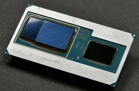
Intel already did this with Kaby Lake-G, but like nobody can buy it. It's also not really a chiplet design, but close enough. I'd be fine using what's in the Xbox Series X or PS5 in a PC setup, if I could buy it for an affordable price. It's not a chiplet design but I'd be up for it. I feel the only reason AMD hasn't pursued this technology for APU's or SOC's is because they don't see it as profitable. They can clearly do it.

8th-Gen-Intel-Core-processor.jpg
 
  • Like
Reactions: ChadD
like this
Their apus already make since so it could potentially make its way into the high end laptop scene.
The problem is the latency introduced by said controller, at their current speeds it’s fine for a CPU but still 3-5 times too slow for a GPU.
 
The problem is the latency introduced by said controller, at their current speeds it’s fine for a CPU but still 3-5 times too slow for a GPU.

If software supports it dual GPU can scale well with a much higher latency.

What they are aiming for is not impossible and can be practical if the moons align
 
If software supports it dual GPU can scale well with a much higher latency.

What they are aiming for is not impossible and can be practical if the moons align
Yeah but it needs developers to have started implementing proper multi GPU code which NVidia and Intel are working closely with developers on. But I haven’t heard of AMD sending out engineering teams like they have to adapt the engines.
 
If they execute this well, it could offer a way to get competitive pricing and performance
 
Why do you guys think this requires anything from developers. This is not a patent for SLI... or anything SLI like.

The OS and developers would be talking to one chip... the controller chip. That is it.

In the same way that a Ryzen CPU shows to the OS and developers as one 16 core CPU... not a dual socket chip.

The only difference between what this patent proposes and current GPUs... is the core complexes are on different silicon. GPUs already have internal core complexes and on die controllers. (believe it or not CUs on todays chips that are far enough apart on the silicon already need smart controllers to not split work to far apart CUs.... and cache systems for different work groups) This patent is for the interconnect technology to move them to their own silicon packages. Yes that creates more latency then the really far apart CUs deal with on the same silicon. However AMD has already shown how they plan to fix that issue with the 6000 cards. More cache. The controller will do the same thing the Ryzen controller does... it will send as often as possible things that rely on each other to the same complex, and direct traffic... and each complex will have likely 2-3x the cache of what the 6000s have is I was guessing.

Considering how hard it is to fab 500mm2+ chips which all GPUs these days are.... even a 4 chiplet + controller chip setup could well double yields. (and yes half costs) AMD could then add a ton more CUs for the price.... or reduce pricing. My guess would be is they increase core count and heavily increase their profit margin. But anyway ya this is NOT SLI or a dual GPU in anyway.
 
This comes as no surprise. Given their constraints amd's production would benefit extremely from a chiplet design, not only for improving yields but likely also for improving the speed at which they could implement new gpu design into their apu's. I imagine it also could help with optimising the apu/gpu/cpu production ratios to market demand.
 
I'm thinking this means Crossfire without the lag. See 3Dfx Voodoo 5-6000 for reference.

The reason 3dfx SLi didn't have frame variance issues is because all cards/chips rendered the entire scene in lock-step, just alternated which cards/chips displayed which scanlines. This was an incredibly wasteful approach that only increased the fill rate, and not the geometry rate of the SLi implementation. Their SLi implementation wasn't without issues though, since it was effectively interlacing, interlace tearing was a problem that could result in a bizarre looking output on the screen, especially if the cards/chips got out of sync. You'd end up with each card rendering different frames and interlacing them together. This problem got worse the higher the effective frame rate was because timing and bus bandwidth became a problem.

Getting any multi-card rendering setup to not have frame variance issues is really an impossible task since both cards are not going to have the exact same load at any given time. There are just too many variables to be able to perfectly sync the rendering output of multiple video chips at once.
 
The problem is the latency introduced by said controller, at their current speeds it’s fine for a CPU but still 3-5 times too slow for a GPU.
GPU's care less about latency than CPU's. This is why GPU's use GDDR memory instead of DDR, because GDDR has much higher latency. Due to the nature of the work load of a GPU, bandwidth is far more important than latency. CPU's have to worry about IPC where GPU's worry about throughput. GPU's don't care what order something is processed as long as it gets done, where for CPU's the order is very important. Cache is the solution to high latency, and that's why modern CPU's have more cache than GPU. It's obviously not a very good solution as it just dominates the CPU die and therefore costs money. This is also why Apple's M1 is able to perform so well because the memory sits right next to the SOC, and therefore doesn't need as much cache. Also why Apple's M1 doesn't have upgradeable memory.

This is why HBM memory is far better for graphics as not only it's mounted very close to the GPU, but it also has a lot more bandwidth. Though it still has higher latency than DDR, like a lot more, which is why this isn't ideal for CPU's. Modern GPU's may begin to need to lower latency as well but like CPU's it can use some cache to fix that. This maybe why AMD and Nvidia are using GDDR6 instead of HBM as not only it's cheaper but the latency is lower as well. Even though HBM is mounted closer to the GPU to reduce latency, and has far more bandwidth, it maybe that these tradeoffs aren't enough to justify the extra cost and complexity of HBM.
 
Last edited:
GPU's care less about latency than CPU's. This is why GPU's use GDDR memory instead of DDR, because GDDR has much higher latency. Due to the nature of the work load of a GPU, bandwidth is far more important than latency. CPU's have to worry about IPC where GPU's worry about throughput. GPU's don't care what order something is processed as long as it gets done, where for CPU's the order is very important. Cache is the solution to high latency, and that's why modern CPU's have more cache than CPU. It's obviously not a very good solution as it just dominates the CPU die and therefore costs money. This is also why Apple's M1 is able to perform so well because the memory sits right next to the SOC, and therefore doesn't need as much cache. Also why Apple's M1 doesn't have upgradeable memory.

This is why HBM memory is far better for graphics as not only it's mounted very close to the GPU, but it also has a lot more bandwidth. Though it still has higher latency than DDR, like a lot more, which is why this isn't ideal for CPU's. Modern GPU's may begin to need to lower latency as well but like CPU's it can use some cache to fix that. This maybe why AMD and Nvidia are using GDDR6 instead of HBM as not only it's cheaper but the latency is lower as well. Even though HBM is mounted closer to the GPU to reduce latency, and has far more bandwidth, it maybe that these tradeoffs aren't enough to justify the extra cost and complexity of HBM.
GPU’s use GDDR and HBM because it can be read from and written to in a single clock cycle unlike DDR which can only do one or the other not both. And you are confusing processing time with latency, latency is only latency when it’s a noticeable problem until then it’s processing time. I don’t know the specifics of the IO controller I only know their past attempts from early 2019 added large processing times as it was batching work between CCX’s and combining the results. This created unacceptable frame time delays, now they may have found a way to fix that since then which would be great.
 
GPU’s use GDDR and HBM because it can be read from and written to in a single clock cycle unlike DDR which can only do one or the other not both. And you are confusing processing time with latency, latency is only latency when it’s a noticeable problem until then it’s processing time. I don’t know the specifics of the IO controller I only know their past attempts from early 2019 added large processing times as it was batching work between CCX’s and combining the results. This created unacceptable frame time delays, now they may have found a way to fix that since then which would be great.
We're talking latency as in the time it takes for memory to move. I don't know how much nanoseconds it takes for each memory standard but as far as I know HBM > GDDR > DDR when it comes to latency. Coincidentally, HBM > GDDR > DDR when it comes to bandwidth. Starting to see a pattern here? It's all about latency vs. bandwidth. CPU's have to process stuff in order, meaning you can't do one thing without doing another first. The quicker one thing gets done, the quicker the next thing can get done. This is IPC. GPU's specialize in stuff that has no order, which means many tasks can be done individually without depending on other tasks to be finished first. CPU's can't do else without doing if first, and can't call other functions without finishing other tasks first. I can't calculate your test score without checking your answers first. GPU's do a lot of math, which has no order that needs to be done. If you physically separate the components then you do have higher latency issues, but this is less of a problem for GPU's because they don't care when it's done so long as it gets done.

Cache fixes this because it's built into the CPU and is super fast in terms of latency. L1 has the lowest latency but also has the lowest amount. L2 has higher latency but has more storage. L3 has the highest latency but also bigger storage. Also cache is smart as it stores frequently used data, including output. Depending on how often it gets used depends on which Level of cache it sits in.
Memory with the CCX IO controller isn’t the issue it’s the time it takes to batch jobs to the various GPU chiplets and recombine their output poling which has what job stack and making sure they are evenly distributed while making sure that jobs are completed in time l. I should have been more clear, the memory itself is mostly negligible.
 
I don't know how much nanoseconds it takes for each memory standard but as far as I know HBM > GDDR > DDR when it comes to latency.
If you can find the actual numbers that would be cool. I know GDDR > DDR for latency, but I've never found the numbers for HBM and so I could not make the assumption that HBM is worse in latency.
 
If you can find the actual numbers that would be cool. I know GDDR > DDR for latency, but I've never found the numbers for HBM and so I could not make the assumption that HBM is worse in latency.
I was going to respond with some long technical babble but this guy here does a better job on the GDDR vs HBM.


As for GDDR vs DDR they have completely different priority sets, DDR is single read or write per clock tick at very low latency, GDDR can read and write per clock tick at faster speeds but has a higher latency. GDDR is going to move large amounts of ordered data quickly in and out simultaneously, while DDR is great at moving lots of small amounts of random data quickly.

This is where concept latency comes in and it is a course topic onto itself and it gets ugly. But from what I know different boards will run slightly different timings so while they give us the final speed they are running at they often don't publish the actual memory timings and you have to get in pretty deep to get the specific numbers but for the most part the latency on a GPU is a non factor because of the huge amount of data it is moving at once.

I started listening to the first few minutes of that video and realized it wasn't getting into any specifics and then started quickly skipping through it.

Did they mention any numbers or did they specifically say that HBM memory has much faster or slower latency vs GDDR or DDR? If so can you give me the timestamp. Thanks.
 
Last edited:
Back
Top