From ATI to AMD back to ATI? A Journey in Futility @ [H]

Considering that's the only reason why you'd add another power connector above PCE-E+6-pin I think it's pretty safe to assume.
While it would SEEM that way yet.. however in actuality PCIe+6 pin cards hardly ever get near 150W...just look at the 1070, (supposedly 150W card) have an 8 pin (225).. then when you look at actual power draw it is not "much more than 150W" (avgs between 145-165W). I guess if ppl are now equate 10% = "much more" then I well../boggle
Point being I don't see the "They are using much more than 150 watts" (emphasis on MUCH MORE), now if it exceeds 185-195..(+30% over TDP) sure.. then we can start on about MUCH MORE..
As noted, with the 1070, the 8 pin deliveres up to 225W in combination with PCIe slot, however just because it is there does not mean it exceeds its suggested TDP by a significant %. Most cards don't event draw even close to max % (75W) through the PCIe slot, iirc its about 35W via PCIe.
 
  • Like
Reactions: NKD
like this
man flipping threw the last two pages of this thread has been a real exercise on what people are willing to say out of emotion and frustration.

The article itself was written out of emotion and frustration. So the thread followed suit. What else was to be expected? lol.

I'm not getting a new card this year, my old 980 will have to do till next year but it's been super fun following this thread. :)
 
Are you still f'in complaining about a card hitting 1.5ghz + for less than 300? Giving you almost fury x performance? Got something else to complain about? If true it's a beast I could care less if it uses 20 more watts. They are saying cards hitting 1.4+ out of the box and 1.5+ with little tweaking.

Can't wait till another post about how this is bad. If I can get a $250 card and clock it faster than fury x, I don't give a shit about extra 20 watts. Oh did you just really complain about hitting 1070 performance for 100 less.

I'm saying it matches what [H] said

]AMD has a problem on its hands, as both these products have come up significantly short of where these were supposed to land. But that is OK for AMD, it will simply send Chris Hook out to fall on the sword and tell a story of that was the plan all along....to produce brand new parts much slower than its last high end GPUs. In the simplest terms AMD has created a product that runs hotter and slower than its competition's new architecture by a potentially significant margin
Now, I am sure AMD will take every step possible to mitigate this gap but the simple reality of the situation as it stands today is that AMD has a loser on its hands and are going to have to pull every trick in the book to spit-shine the turds, and the fact of the matter is pricing is how you do that.

But I'll welcome price pressure on Nvidia happily as it means I can buy good gpus cheaper ;)
 
I'm saying it matches what [H] said


But I'll welcome price pressure on Nvidia happily as it means I can buy good gpus cheaper ;)
Hard put it in the most negative way you can imagine. To me it seems one hell of a product for the price. H would get credit if AMD ever stated in the last year that Polaris was a super high end chip. It never was. Obviously it would be slower than nvidia high end chips. So that was evident. AMD always said main stream and priced it better than people thought. It was more a preemptive strike against this launch than anything. Yea it may be a little hot and use a little more wattage cuz it's a denser chip. So what. If I can get it for 250 and it overcome decent and gives me 980ti performance or above. I am likely to push it to its highest limit. If stock cards OC to 1400 and within 150w envelope that's already sweet enough.
 
  • Like
Reactions: Zuul
like this
i noticed that AMD only have mention TBP, while allmost evry tech site say same number as TDP. You are the first that actually point that out, see i do learn a littel from reading your posts.


Did you see their comparisons of the 270x?

They are using Max power usage of the 270x vs the TDP of the rx470 or something like that what does that tell you? They aren't being straight forward about their power consumption figures at all.

LAST 2 gens AMD has gone to use TBP instead of TDP since their cards were going pretty crazy over TBP (TDP would be higher if they wanted to use that it would have made their cards look really bad).

Now what they are doing is mixing the two together and adding Max power usage when comparing to older cards, to make their cards look "better" in the short term before reviews come out.

All of this wish washy crap AMD is doing doesn't give me any confidence. Either they have it where it counts or they don't, and so far the performance expectations have dropped for me from 4 months back, and now they aren't telling us anything concrete like power consumption? When was the last time we saw AMD being all mysterious about stuff like this? Hmm Fury comes to mind.
 
Well Nvidia cards are being reduced dramatically, if the 480 really performs well as in 980+, then all those 980's and below will need to be sold less than $200 or gather dust maybe. Man, you can win at each market segment, as in AMD can win big in the less than $300 club. Look at Nvidia in the Mainstream market - take that away and give it to AMD and who will be the real winner? Still two things I see - perf/$ that is very good and quantity of cards that people can purchase. Giving the AIBs ability to improvise and stand out can only help. OCing tools also sound fun as well.

The high end is Vega and HBM2 at which the 1070/1080 will probably move to performance cards vice Ethusiast cards - Well time will tell rather quickly I say.
 
  • Like
Reactions: NKD
like this
Did you see their comparisons of the 270x?

They are using Max power usage of the 270x vs the TDP of the rx470 or something like that what does that tell you? They aren't being straight forward about their power consumption figures at all.

LAST 2 gens AMD has gone to use TBP instead of TDP since their cards were going pretty crazy over TBP (TDP would be higher if they wanted to use that it would have made their cards look really bad).

Now what they are doing is mixing the two together and adding Max power usage when comparing to older cards, to make their cards look "better" in the short term before reviews come out.

All of this wish washy crap AMD is doing doesn't give me any confidence. Either they have it where it counts or they don't, and so far the performance expectations have dropped for me from 4 months back, and now they aren't telling us anything concrete like power consumption? When was the last time we saw AMD being all mysterious about stuff like this? Hmm Fury comes to mind.
Lets wait until the reviews come out. Because its 50/50. Amd hasn't really been deceptive. It's just everyone thinking all possible scenarios and making things up. It may not be as power effiecient as pascal but I don't think it will be that bad since amd limited it to 150 TDP. It remains to be seen.
 
These partner cards will have more than a 6 pin power connector ;) They are using much more than 150 watts.


Well thats a given. If its less than a power hungry 290x, I'm good. I have a 1kw PSU. Surface die area is going to be the issue when cooling these. Its an issue by the process technology and not necessarily the design.
 
OC3D :: Article :: AMD are planning to provide better overclocking support with Polaris :: AMD are planning to provide better overclocking support with Polaris

Fury X has disappointingly low overclock potential because it was clocked close to it's limit out the box. Not because of voltage control lol. Seriously, anyone with 1200mhz on a Fury X (14%) basically celebrated the achievement as if they had just witnessed the return of Cthulu.
Isn't this just API or some such? I recall it was not possible to tweak voltage of FuryX for several weeks after launch. If so, good news, but nothing telling about performance.
 
That i didnt quite get, i meen you been pointing out lots of time you dont belive TDP is 150w, but round TDP 130w, wich i think ur right, well becouse AMD only told TBP, if TDP for 470 is 110w, both 470 and 480 has according to the firestrike benches 1266 as boost clock, since they same chip, same mhz, 470 some cut, will there be big diffrence in consuption.

Ask, becouse you know this stuff 100 times better than me.


I still think the 480 will use around 130 watts, actually now I'm thinking it can be higher because of the way AMD just isn't coming out and saying it, it is concerning to me. Just like the way the performance seems to be going down I have a feeling their perf/watt numbers are done the same way to confuse potential buyers. 130 watts is decent for a mid range board, but it doesn't look that good when you look at a 1070 which uses 150 watts and has much more performance. This is the only explanation I can think of why AMD beating around the bush with its perf/watt figures and power draw for the card.

At this point there needs to be no need for all this, Pascal is out, everyone knows what it is what it can do, yeah the 1060 isn't there yet, but come on, its pretty easy to extrapolate what the 1060 can be like even if it doesn't match the 1080 perf/watt, we can still understand its going to be less than 150 watts with 980 performance levels easily.
 
Well maybe AMD is trying to have cake and eat it too. In other words sell energy efficient, cooler cards much better performance cards then previous generation but allow higher performance but with much more power/heat. Win/Win. AMD needs to get the buyers to be their best communicator and seller shouting from the roof tops. That if sorta accomplished will move more cards then anything else.
 
=-0
2.2 is pretty much max for AIB's with the 2 8 pin power connects.

Galax GeForce GTX 1080 HOF hits 2.2GHz on air, 2.5GHz on LN2 - Graphics - News - HEXUS.net

2.2 on air.
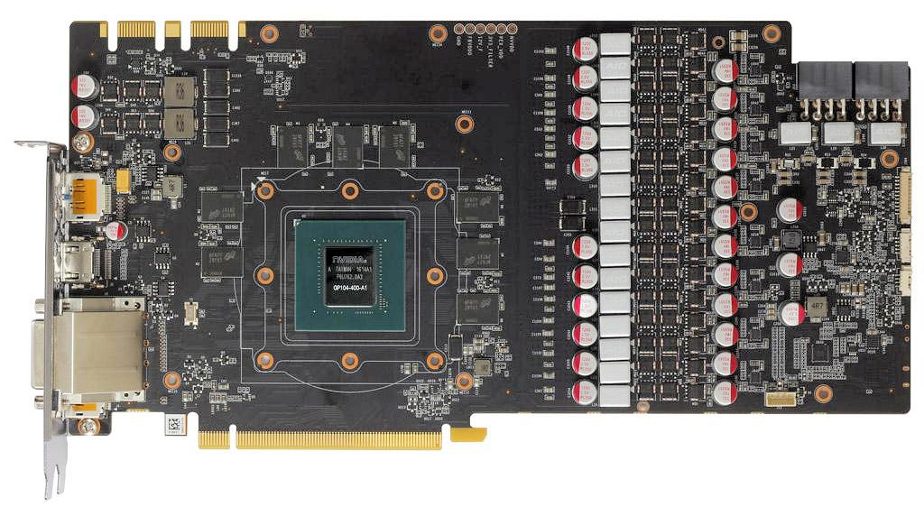
of course forgetting (conveniently) to mention this is a completely custom PCB with digital VRMS (8+2 phase vs 1080 ref 5+1).. whats next citing the ZOTAC PGF as the normal power delivery for AIBs

REF:
upload_2016-6-17_9-4-8.png
CUSTOM:
upload_2016-6-17_8-59-20.png

Then again, just because is custom doesn't mean much
ASUS ROG STRIX GeForce GTX 1080 offers poor overclocking | VideoCardz.com
or that AIBs have to "cheat"
MSI and ASUS Send VGA Review Samples with Higher Clocks than Retail Cards

but I must digress this is off topic and if Mods feel need to move post to appropriate thread , please do
 
I still think the 480 will use around 130 watts, actually now I'm thinking it can be higher because of the way AMD just isn't coming out and saying it, it is concerning to me. Just like the way the performance seems to be going down I have a feeling their perf/watt numbers are done the same way to confuse potential buyers. 130 watts is decent for a mid range board, but it doesn't look that good when you look at a 1070 which uses 150 watts and has much more performance. This is the only explanation I can think of why AMD beating around the bush with its perf/watt figures and power draw for the card.
You tell me AMD has smarten up some and keep things like jello against a wall :LOL:. All they say is 2.8xperf/watt. Looks like AIBs can have some rather power soaking cards released if they want to - hence AMD keeping quiet allows more flexibility and not countless ridicule because they say one thing and it turns out to be false.
 
  • Like
Reactions: NKD
like this
=-0

of course forgetting (conveniently) to mention this is a completely custom PCB with digital VRMS (8+2 phase vs 1080 ref 5+1).. whats next citing the ZOTAC PGF as the normal power delivery for AIBs

REF: CUSTOM:
Then again, just because is custom doesn't mean much
ASUS ROG STRIX GeForce GTX 1080 offers poor overclocking | VideoCardz.com
or that AIBs have to "cheat"
MSI and ASUS Send VGA Review Samples with Higher Clocks than Retail Cards

but I must digress this is off topic and if Mods feel need to move post to appropriate thread , please do


The original comments that leaded to that specific post, weren't OT, so .........
On one hand, if it's true, it's a little concerning for power consumption. On the other, it seems that at least P10 can actually do something with extra power, where Pascal....hasn't.

And since when did the world go nuts about a ~15% OC? Edit: percentage

.....if you have a problem with my post, have a problem with his too.

I did say AIB I didn't specify board but that is included.
 
whats interesting to me was the accusation that "Amd had a top tier chip". What chip designer in the world thinks that moving from a 596mm2 chip down to a 232mm2 chip even with a node shrink is going to equal a much faster chip? It's ridiculous.
 
whats interesting to me was the accusation that "Amd had a top tier chip". What chip designer in the world thinks that moving from a 596mm2 chip down to a 232mm2 chip even with a node shrink is going to equal a much faster chip? It's ridiculous.


First off they never moved a 596mm2 chip to 232mm2, they moved a 438mm2 chip to 232mm2. And this is more than just one die shrink. We are talking about a half node to a half node, but the changes with planer to finfet should garner more then a traditional node shrink.

Which chip designer you ask, the same one that created 4xxx line, they were able to do it in the past, but not this time.
 
Then AMD slides put reference clocked at 150W max - let's be generous and say 130W - the moment we start touching voltage overclocking power consumption increases greatly so we will be looking at 180? 200? W part to match performance of stock 1070
This. Until we see real reviews, it is obviously pure speculation, but …

It seems AMD has learned its lesson from 290X days. Back then they released effectively OC’d card performing on the peak of its abilities, and with crappy cooler to boot. That immediately got bad reputation, very similarly to GTX480.

Now, they probably started hitting FinFet thermal wall, and so they decided to release slower card, but with nice other characteristics (power, heat, noise). And with that, and good price, and improved driver support, AMD will get what they need most: good reputation. As long as RX480 has reputation of fast card on its pricepoint, that is silent and will not suck entire nuclear powerplant, it should get good reviews, good reputation, and sell well. And selling well = good DX12 support = great starting point for Vega.

Then it will be to AIB partners to prepare factory-OC cards with beefy and silent cooling, that will (hopefully) threaten 1070 at substantially lower price point, though with higher power bill and lower OC potential.

But why sell the base version $199 cheap? Probably because it still can be profitable to them: It is a small chip, and thanks to PS4 Neo, they need to produce it in large quantities. They will also have lot of dies to choose from (they are harvesting to 470, and also to lower-clocked PS4 Neo). Which nicely solves for them minimum wafer order from GloFo that was hurting them in recent years.
 
First off they never moved a 596mm2 chip to 232mm2, they moved a 438mm2 chip to 232mm2. And this is more than just one die shrink. We are talking about a half node to a half node, but the changes with planer to finfet should garner more then a traditional node shrink.
FuryX, which is their fastest, is 596mm2.
 
whats interesting to me was the accusation that "Amd had a top tier chip". What chip designer in the world thinks that moving from a 596mm2 chip down to a 232mm2 chip even with a node shrink is going to equal a much faster chip? It's ridiculous.
I mean, nV did pull off a de-facto ~250mm^2 die having performance of full 600mm^2 die.

AMD could expect to do so too, especially since Fury X was frankly... not that great.
 
whats interesting to me was the accusation that "Amd had a top tier chip". What chip designer in the world thinks that moving from a 596mm2 chip down to a 232mm2 chip even with a node shrink is going to equal a much faster chip? It's ridiculous.
Well, going from 28nm to 14nm in theory lets you get the same number of transistors in 1/4 of the die area. If you can also gain some MHz you can build a chip with more transistors that runs faster, yet still has a much smaller die while performing better.
 
Well, going from 28nm to 14nm in theory lets you get the same number of transistors in 1/4 of the die area. If you can also gain some MHz you can build a chip with more transistors that runs faster, yet still has a much smaller die while performing better.

Let me guess. You're thinking 1/2 the gate width, so 4x the density?

That's not how it works D: starting with the fact that 14/16/28 doesn't refer to gate width, it doesn't refer to anything meaningful really
Feature sizes on Intel’s 14nm process compared with its 22nm process are:

42nm fin pitch, down .70x

70nm gate pitch, down .78x

52nm interconnect pitch down .65x

42nm high fins, up from 34nm

a 0.0588 micron2 SRAM cell, down .54x

~0.53 area scaling compared to 22nm

As we have come to expect these days, there’s nothing in a 14nm process that measures 14nm.
 
They could also be shorting it, although (IMO) that is foolish immediately preceding a major launch that looks to be quite strong.

But actually an analyst firm upgraded the stock from "Beware, there be serpents here" to "Somewhat dangerous". That's why it went up.

Regarding that Galax 1080, I'll believe it can hit 2.2Ghz on air when anybody outside Galax gets one and tests it.
 
Let me guess. You're thinking 1/2 the gate width, so 4x the density?

That's not how it works D: starting with the fact that 14/16/28 doesn't refer to gate width, it doesn't refer to anything meaningful really
Well, I said theoretically. And, I'm not sure how showing that Intel got about half going from 22 to 14nm proves that AMD couldn't go from 28 to 14 and get a much smaller die that clocks higher and end up running faster. 28->14 should show greater gains than dividing the die size by two, though obviously dividing by 4 isn't going to be realizable.
 
This. Until we see real reviews, it is obviously pure speculation, but …

It seems AMD has learned its lesson from 290X days. Back then they released effectively OC’d card performing on the peak of its abilities, and with crappy cooler to boot. That immediately got bad reputation, very similarly to GTX480.

Now, they probably started hitting FinFet thermal wall, and so they decided to release slower card, but with nice other characteristics (power, heat, noise). And with that, and good price, and improved driver support, AMD will get what they need most: good reputation. As long as RX480 has reputation of fast card on its pricepoint, that is silent and will not suck entire nuclear powerplant, it should get good reviews, good reputation, and sell well. And selling well = good DX12 support = great starting point for Vega.

Then it will be to AIB partners to prepare factory-OC cards with beefy and silent cooling, that will (hopefully) threaten 1070 at substantially lower price point, though with higher power bill and lower OC potential.

But why sell the base version $199 cheap? Probably because it still can be profitable to them: It is a small chip, and thanks to PS4 Neo, they need to produce it in large quantities. They will also have lot of dies to choose from (they are harvesting to 470, and also to lower-clocked PS4 Neo). Which nicely solves for them minimum wafer order from GloFo that was hurting them in recent years.


PS4 neo is not the same chip, PS4 neo is an semicustom, with both a CPU and GPU integrated into one chip.
 
Isn't pascal 312mm2? Or something like that. How is that defacto 250mm2?

16nm and 14nm have transistor density differences, you can't compare these nodes like that, even if they were the same densities you can't compare different Fabs like this......

Apples and oranges.
 
Well, I said theoretically. And, I'm not sure how showing that Intel got about half going from 22 to 14nm proves that AMD couldn't go from 28 to 14 and get a much smaller die that clocks higher and end up running faster. 28->14 should show greater gains than dividing the die size by two, though obviously dividing by 4 isn't going to be realizable.


mask layers of GF and Samsung 14nm are still at 20nm. One of the differences (the major one) from Intel's 14nm to what AMD is using.
 
N
16nm and 14nm have transistor density differences, you can't compare these nodes like that, even if they were the same densities you can't compare different Fabs like this......

Apples and oranges.
not apples and oranges. Fuji apples vs Granny Smith. So very slightly different, and both apples.
 
Well, I said theoretically. And, I'm not sure how showing that Intel got about half going from 22 to 14nm proves that AMD couldn't go from 28 to 14 and get a much smaller die that clocks higher and end up running faster. 28->14 should show greater gains than dividing the die size by two, though obviously dividing by 4 isn't going to be realizable.

That's not how it works. There's nothing '14nm' about the process. This is 20nm FinFet.

Before it was 28nm FD-SOI planar.
 
N

not apples and oranges. Fuji apples vs Granny Smith. So very slightly different, and both apples.


Just transistor density alone its 10% or so different, so in theory if nV's chip was done on 14nm GF, it would have a chip size of 270mm, and this is all without looking at AMD chips/ALU's tend to take up less space as they are denser than nV's.
 
Whenever something is hyped this hard for this long before actual product shows up it can only mean one thing. It's a turd. Obfuscate everything about it and try to make as many people as possible believe it's the second coming before it shows up so they buy it before they find out it's crap. Classic marketing strategy when dealing with a poor product. AMD gave themselves an entire month from announcement to NDA expiration to build hype. I's because they don't have anything of substance to show.
 
Then why is it called 14nm?

The name means little, its just marketing. If you look at many nodes in the past and compare them across fabs, you will see there are many differences but they end up with the same names.

14nm from GF/Samsung is a half node. Intel is a Full node change.

The reason why they are both called 14nm is the transistor size. But inherent to Intel's process, their mask and metal layers are also 14nm while GF/Samsung's are not.
 
Then why is it called 14nm?

Quite literally to distinguish it from 20nm Planar. The marketing people thought "well if we call it 20nm (which also has no bearing on any physical sizes btw) people will think it's the same as 20nm planar" so they decided to call it 14nm to convey the technological advancement to the average consumer
 
Back
Top