AMD EPYC Rome 64-Core Server Versus Intel Dual Socket Xeon Platinum Benchmark

cageymaru

Fully [H]
Joined
Apr 10, 2003
Messages
22,076
HotHardware has video of the C-Ray raytracing benchmark shown at the AMD Horizon Event. The AMD exhibit demonstrated just how powerful the new 7nm EPYC Rome architecture is with its new chiplet design that was leaked by AdoredTV. An Intel 8180M dual socket Xeon Platinum CPU server with 56 cores total and 112 threads was matched against a single AMD Zen 2 EPYC Rome 64-core CPU based server. Needless to say, the 7nm AMD EPYC Rome CPU easily won the battle. AMD CEO Dr. Lisa Su says that the 7nm EPYC Rome CPU will be a 64-core, 128-thread processor. The entire slideshow can be viewed here. Thanks juanrga !


In addition, AMD has been able to add some security enhancements with Zen 2 as well, including hardware mitigation for recently discovered Spectre CPU vulnerabilities. AMD has also increased the number of encryption keys for virtualization to allow companies to support more virtual machines. Infinity Fabric is now in its second generation, and I/O per die has been optimized to improve both latency and power. While Infinity Fabric itself is being kept on a 14nm process, the accompanying chipset for Zen will be built on 7nm.
 
Is this correct / true?

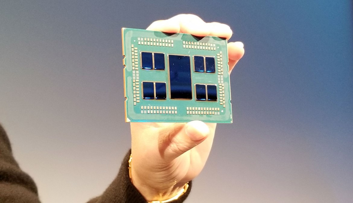
If you look at the CPU there is a huge 14nm section in the middle and 7nm cores around it.

amd-next-horizon-Chiplet_design.jpg

big_amd-epyc-zen-2-64-core-cpu.jpg.jpg
 
Is this correct / true?
Yes. They explained that they can't shrink the 14nm I/O and analogue circuits as much as the other digital circuits which mostly consist of the rest of CPUs .
It also frees up die space for CPU cache on chiplets. These should be quite fast..and extremely efficient.
 
Yes. They explained that they can't shrink the 14nm I/O and analogue circuits as much as the other digital circuits which mostly consist of the rest of CPUs .
It also frees up die space for CPU cache on chiplets. These should be quite fast..and extremely efficient.

I'd put good money that the CPU chips are just 7nm ryzens with functionality fuzed off. This allows them to strip functionality off of the base ryzen die (1 off chip I/O block that is PCIe in desktop and hub link in server, simplified memory controller, etc) thus reducing desktop costs and having better overall binning options. Very little point in doing two separate 8C die designs for them between desktop and server.
 
I'd put good money that the CPU chips are just 7nm ryzens with functionality fuzed off. This allows them to strip functionality off of the base ryzen die (1 off chip I/O block that is PCIe in desktop and hub link in server, simplified memory controller, etc) thus reducing desktop costs and having better overall binning options. Very little point in doing two separate 8C die designs for them between desktop and server.
They wouldn't separate the designs at all for the chiplets, could just use a smaller IO chip for desktop.
One thing they did mention was using different processes for different chips, e.g. LP or HP versions. That will be amazing for laptops and maybe even for high end if they go for that part of the workstation/HEDT market.
7nm zen must be quite a decent re-design, doubt it's a shrunk zen core. Wrong shape to boot and too small, they shaved it and made the cache in the middle, it's the only way they can get the 8core CCX going.
 
I'd put good money that the CPU chips are just 7nm ryzens with functionality fuzed off. This allows them to strip functionality off of the base ryzen die (1 off chip I/O block that is PCIe in desktop and hub link in server, simplified memory controller, etc) thus reducing desktop costs and having better overall binning options. Very little point in doing two separate 8C die designs for them between desktop and server.

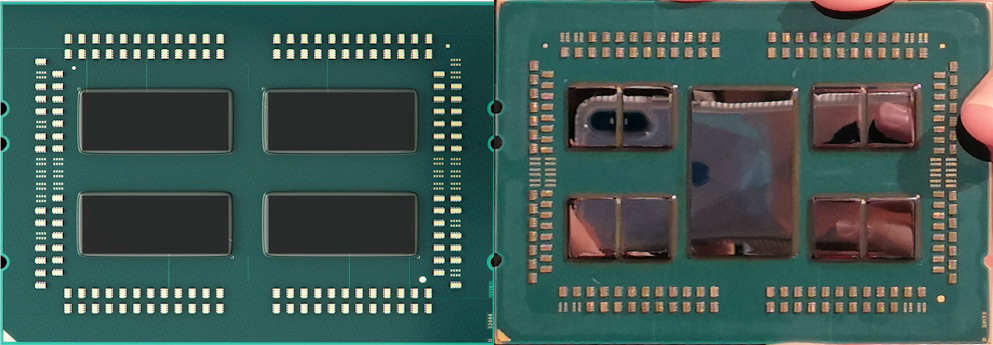
Here you go, clearly cut most of the die off for these chiplets. Even though density is 2x, it takes often more transistors to make the same thing at a smaller node.
epyc vs epyc 2.png
 
If someone came to [H] back in 2013-ish and said that's how things would be going down in 2018 for AMD, what would he get?

yes... an unmesurable amount of dee-doo.

This is just amazing.
 
So it looks like a 16 core Zen2 design is a go? I wonder if it will be the same MCM design or a monolithic design, they did mention something about 2 different strategies I believe. If they can release a 16/32 mainstream chip with decent clocks, man...amazing!

A 2S server with 128/256 worth of processor is a little mind blowing. The top Intel solution will be 96/192 and likely clocked lower because of the 14nm design, but this requires a whole new socket. Man AMD is killin it on the CPU front these days...Love that they can beat a 2S Platinum setup with a single socketed chip. Rome shaping up to be a huge disrupter, this is where the industry wakes up to AMD I think.

Also, Threadripper 3950X inbound? (y) I smell a new rig in the making!
 
It's also incredible to see how spinning the fabs out turned out for them. That was considered a massive mistake back when it happened - and it was in some ways, GloFo exclusivity and so on - but with the right strategy, it means they're nimble and can focus on making kickass chips. All the while Intel struggles with... yeah.

I've said it before, but it bears repeating... welcome back, AMD!
 
Here you go, clearly cut most of the die off for these chiplets. Even though density is 2x, it takes often more transistors to make the same thing at a smaller node.
View attachment 118145

It does not generally take more transistors to do the same thing, rather the design of transistors needs to be completely changed, and often the extra shrinkage is used to fill in more architectural 'fattening', but yes, I agree with you that those chiplets are most likely free of I/O and other bloat, and the only way we'll see these little guys on a desktop CPU is with a separate I/O controller chip like in Rome.
 
Last edited:
People were making fun of me for picking up AMD @ ~$3/share just a few years ago.

Good times ahead it seems.

I was kicking myself for not having any spare money to do so just out of principle. You know, keep the underdog floating and all, even though they were pumping out mostly junk.

I am not getting any profit, but it's hard to not get all warm and fuzzy when a turnaround like AMD happen. I can't wait to reach the point in which I can build a brand new rig, because I'll go full retard on two AMD beasts, one for me and one for my wife, celebrating all the K6s, Athlons and Durons that served me so well in the past!

Now, if they manage to pull that on the GPU front as well, that'll be massively EPYC indeed!
 
Last edited:
Here you go, clearly cut most of the die off for these chiplets. Even though density is 2x, it takes often more transistors to make the same thing at a smaller node.
View attachment 118145

Um, your photo says literally nothing. They are two completely different processes from 2 completely different companies with completely different physical design constraints and thus physical design. Anyone trying to base what's on the new one off of the physical size of the old one is at best guessing.
 
Um, your photo says literally nothing. They are two completely different processes from 2 completely different companies with completely different physical design constraints and thus physical design. Anyone trying to base what's on the new one off of the physical size of the old one is at best guessing.
Well, their guess is as good as yours....
imho, if a separate i/o chip adds minimal latency, then there is zero reason not to and just about every reason to share chips between server and desktop like they have been. The exception would be to add more than 8c per die, but I see no reason that couldn't be shared too, although they'd probably limit it to the high end desktop chips.
 
Last edited:
Oh man, can't wait for this to trickle down into Zen 2. 1700 is feeling long toothed.
 
It's also incredible to see how spinning the fabs out turned out for them. That was considered a massive mistake back when it happened - and it was in some ways, GloFo exclusivity and so on - but with the right strategy, it means they're nimble and can focus on making kickass chips. All the while Intel struggles with... yeah.

I've said it before, but it bears repeating... welcome back, AMD!

personally i think a lot of credit has to go to Lisa Su.. i honestly don't think AMD would be where it's currently at without her.
 
personally i think a lot of credit has to go to Lisa Su.. i honestly don't think AMD would be where it's currently at without her.

For sure, Lisa Su has done a great job turning things around. Some credit probably also goes to Jim Keller who seems to have a golden touch (K8, Apple chips, and Zen). Now that Intel is struggling, guess who they've hired...
 
For sure, Lisa Su has done a great job turning things around. Some credit probably also goes to Jim Keller who seems to have a golden touch (K8, Apple chips, and Zen). Now that Intel is struggling, guess who they've hired...

true.. that's also the beauty of being an independent contract engineer, get to pick and choose who you work with and make bank in the process.
 
interesting chip design, there was talk about something like this a while ago where the "CPU" circled around what is essentially the IO.

I doubt this thing will sip power though, that IO package is absolutely massive.
 
Lisa Su in that video reminding the guy "But [dont say] the freqeuncy!" was pretty hillarious.
 
Last edited:
Lisu Su in that video reminding the guy "But [dont say] the freqeuncy!" was pretty hillarious.

it was actually meant to be a joke, but i was really hoping after she finished talking she was going to say "oh yeah i almost forgot it was running and so and so Ghz" just to troll the reporters.
 
I am interested how everything is interconnected. Do each pair of chips communicate together? Do they each have access to a pair of DDR channels as a priority? A deep dive is going to be very interesting.
 
I am interested how everything is interconnected. Do each pair of chips communicate together? Do they each have access to a pair of DDR channels as a priority? A deep dive is going to be very interesting.


definitely worth watching, he refuses to go deeper into architecture but still gives hints through various questions about how rome works..

also i want to see that 2P rome system running with 256 threads.
 
Back
Top