No sorry, you'd have to email the folks at either Tech Report or Beyond 3D, as it looks to be custom code. I just remember this article because it's one of the few that actually tested the effectiveness of delta color compression (in an outrageous case Ill grant).
 
And yet again this DOES NOT explain the performance margins shrinking at 4K. You can't say "it's bandwidth-limited" when both cards have 'the same' bandwidth.

If you don't understand how a GPU works, and how RELATIVE performance works, then this thread is pointless for you. You alsoneed to be able to spot outliers in data sets: if you trust everything people tell you with no filter on, then you're going to get a lot of lies :D

Also, the reason Fiji stands pout at 4k is because:

1, The GTX 980 Ti is bandwidth-limited. It doesn't have enough bandwidth to exercise all 96 of those ROPS at 4k, even with the compression!

2. The Fury X is likely ROP or bandwidth-limited. I claim this because the performance rises from 15% versus the 390X at 1080p to 25% over the 390X at 4k.

The card has exactly the same number of ROPs, and 33% highr bandwidth, both possible limits here. But the card has an on-paper advantage of texture and compute throughput of about 40% and 50% respectively. So it's nowhere near it's potential in that regard.

The confusion on Fury X comes because at lowers resolutions it's been CPU-limited in DX11 games. Until we all convert over DX12, it will not have it's moment to shine in CPU-limited situations.
 
Last edited:
I think we're getting off-topic, the original claim was that the Fury X excels at 4K due to HBM:

"And the fact that a FuryX can actually BEAT a 980Ti in 4K gaming, but not 1080 or 1440 gaming shows that the 980Ti runs into a memory bandwidth bottleneck much faster than the Fury X. HBM is performing some sort of Voodoo there."

Both this post and the numbers I posted previously disagree with that claim.
The point here is to show that AMD's increased performance at higher resolutions is not exclusively due to memory bandwidth.


And yet again this DOES NOT explain the performance margins shrinking at 4K. You can't say "it's bandwidth-limited" when both cards have 'the same' bandwidth.

Bottlenecks shift depending on the application, application settings, and hardware. Bottlenecks can shift with in the same frame too (IE first half of the frame can be bandwidth limited, the second half can be shader limited). Defaultluser is correct in his assessments.

Think about this, if we were playing a FPS, open field not too many trees, the top half of the frame could be pixel limited while the bottom half is geometry limited.
Of course, I was just curious if there's anything we can specifically point to about GCN that would explain why it's faster than Kepler (or Maxwell) at higher resolutions. I don't think explaining why Kepler/Maxwell is superior at 1080p really answers that question.

The TPU benchmarks are an average of about 10-15 games, so it's consistent.
 
ah ok, sorry wasn't sure where you were coming from, or I'm reading things wrong, had a bit to drink ;) 1080p doesn't stress the shader performance of these cards at all, so other components will take more affect. At 4k I think the reason why AMD has an advantage is pixel shading power of their cards along with the bandwidth advantage.
 
ah ok, sorry wasn't sure where you were coming from, or I'm reading things wrong, had a bit to drink ;) 1080p doesn't stress the shader performance of these cards at all, so other components will take more affect. At 4k I think the reason why AMD has an advantage is pixel shading power of their cards along with the bandwidth advantage.

I agree that the shader load goes up with resolution (just like everything else), but I find your post confusing. Wouldn't the shader load be exactly the same at 1080p as it is at 4k if you are not CPU-limited?

I think what you really mean to say is you're often CPU-limited at 1080p, so the card isn't as stressed?

The only thing that should INCREASE shader load relative to other functional units is if you turn up the shader effects, right?
 
Last edited:
I agree that the shader load goes up with resolution (just like everything else), but I find your post confusing. Wouldn't the shader load be exactly the same at 1080p as it is at 4k if you are not CPU-limited?

I think what you really mean to say is you're often CPU-limited at 1080p, so the card isn't as stressed?

The only thing that should INCREASE shader load relative to other functional units is if you turn up the shader effects, right?


Shaders (mostly) operate per-pixel. Which means if you have a basic SM2.0 shader running 64 instructions, its running 64 instructions per pixel that the shader is present. So, if you have a piece of geometry that takes up 25% of the screen, it will require a LOT more calculations at 4K than at 1080p. Mind you, some modern shaders run upwards of 200 linear instructions per pixel.

Things like texture draws and geometry calculations dont require NEARLY as much power when you increase resolution. LOD values and dynamic tessellation will increase the load a bit, but in reality, Mesh A rendered in wireframe at 1080p will not be that much harder to render at 4K (in theory), as soon as you slap on a shader-based material, that mesh becomes 4x more complicated to render at 4K versus 1080p.

Add in screen-space post-process effects, and you can see the per-pixel nature of modern graphics ballooning out in 4K.
 
Shaders (mostly) oper
ate per-pixel. Which means if you have a basic SM2.0 shader running 64 instructions, its running 64 instructions per pixel that the shader is present. So, if you have a piece of geometry that takes up 25% of the screen, it will require a LOT more calculations at 4K than at 1080p. Mind you, some modern shaders run upwards of 200 linear instructions per pixel.

Things like texture draws and geometry calculations dont require NEARLY as much power when you increase resolution. LOD values and dynamic tessellation will increase the load a bit, but in reality, Mesh A rendered in wireframe at 1080p will not be that much harder to render at 4K (in theory), as soon as you slap on a shader-based material, that mesh becomes 4x more complicated to render at 4K versus 1080p.

Add in screen-space post-process effects, and you can see the per-pixel nature of modern graphics ballooning out in 4K.

But that's why I made the point in my post: if you are not CPU/geometry-limited at 1080p, the graphics card will draw just as many pixels as it does at 4k. It will just draw them four times as quickly.

The number of pixels having the shader effect applied remains 25%. IF you're rendering 4x as many frames, you're just spreading out the shader operations over time. The shader load should be identical, right?
 
But that's why I made the point in my post: if you are not CPU/geometry-limited at 1080p, the graphics card will draw just as many pixels as it does at 4k. It will just draw them four times as quickly.

The number of pixels having the shader effect applied remains 25%. IF you're rendering 4x as many frames, you're just spreading out the shader operations over time

KINDA.

lets say you have a scene that is roughly 2.5 million triangles, has 1k individual objects, and 50 samples of animation. All of this renders on the card per-frame.

If you render this scene at 1080p four times, you have to render 10 million triangles, 4k individual objects, 200 samples of animation and 12 million total pixels.

If you render this scene at 4K once, you only render 2.5 million triangles, 1k individual objects, 50 animation samples and 12 million total pixels.

So rendering the a scene at 1080p four times actually requires MORE effort than rendering the same scene once at 4K IN THEORY. However, if your card is REALLY good at shader calculations versus another, it will pull ahead more noticeably at higher resolutions, as shader calculations become proportionately MORE of the workload. If your card is much better at geometry and Out Of Order instructions, then it will rock more at lower resolutions, where that extra non-pixel load is actually higher.
 
Okay yeah, I guess razor was implying that geometry would no-longer be the limiting factor as resolution increased, just wasn't clear from his original post. Thanks!
 
Fury X is NOT ROP limited. It is GEOMETRY LIMITED.

Look at the [H] review, and the fillrate numbers. Fury X DOMINATES == NOT a ROP issue. Fury X (and GCN in general but especially Fiji) is very Geometry limited. THAT is the bottleneck, not the ROP's. I have noticed that they are emphasizing geometry improvements in Polaris, so hopefully this will not longer be an issue w/AMD cards.

Geometry isn't really specified with metrics, while ROP's are. This makes them much easier to blame... Hey THIS GPU has less/more ROP's than THAT GPU. Can you directly compare them? No, I don't think so. I think you need to look at their performance, and not just how many there are. I mean, this is no different than anything else. You can't directly compare AMD shader counts to nVidia shader counts, or AMD x86 core counts vs Intel core counts, etc. You gotta dig in...
 
Last edited:
Fair point. I think Raw Bandwidth is really the hero of high-resolutions, which is why HBM is so important to the 4K age. If you can get the same bandwidth out of GDDR, then there should be no HBM advantage.
Although according to that chart a 380x is nearly the same performance as a 390........
Hmm... :)
Look at both the 380x and the 390 at 1440p and then 4k.
That is not right considering how the 390 and 390x are probably one of the best models AMD currently sells in terms of performance (and can be close to Fury in some games).

A better test IMO is like what PCGameshardware.de do where they use various AIB overclock models from both AMD and NVIDIA, this makes more sense as it is closer to what customers would purchase unless they want to buy the very 1st release of cards.
Hitman 2016 PC: DirectX 11 vs. DirectX 12 - Benchmarks: DX12 als Prozessorentlaster [Update 3]
Here they could not even test the 380x beyond 1440p lol.

Edit:
I notice DefaultUser sees the same thing.
Cheers
 
not so sure, i dont expect gp104 to outperform a 980ti at 1500
Yeah the 980ti is probably the only card not crippled in some way.
I could not bring myself to buy either the 970 or 980, but if the GP104 has a 384-bit bus or better and the architecture enhancements seen with GP100 then it would be a great replacement at 980 level.

Saying that, IF they do those improvements then the GP104 would close the gap a fair amount though and would reduce the value of the 980ti cards.
A big IF though :)
Glad I am not in that situation myself.
Cheers
 
So, did we learn anything today about when pascal cards will be out?
From what I can gather it's still looking like June.
 
So, did we learn anything today about when pascal cards will be out?
From what I can gather it's still looking like June.

All of my 25 years experience following the GPU circuit point to later this year, late Q3/early Q4.

- HDM2 supply isn't there yet
- GM200/GM204 are still selling well
- Little pressure yet from the competition
- NVDA's marketing machine hasn't ramped up for Pascal
- This thread hasn't reached 1000 posts yet (only half kidding here. NVDA absolutely watches threads like this to see when stuff hits fever-pitch and will time marketing releases/"leaks" and possibly launch accordingly) :)

But it's a fun exercise thinking that Pascal is coming sooner, which is why most of us keep coming to this thread.
 
Last edited:
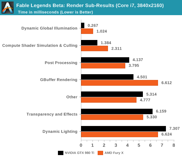
Fury X is NOT ROP limited. It is GEOMETRY LIMITED.

A good indicator for geometry performance is the gbuffer pass. Here we see fury x falling behind in fable legends.

KLlrSA.png


Fable Legends Early Preview: DirectX 12 Benchmark Analysis
 
I agree that the shader load goes up with resolution (just like everything else), but I find your post confusing. Wouldn't the shader load be exactly the same at 1080p as it is at 4k if you are not CPU-limited?

I think what you really mean to say is you're often CPU-limited at 1080p, so the card isn't as stressed?

The only thing that should INCREASE shader load relative to other functional units is if you turn up the shader effects, right?


Like what others have stated, each pixel needs one extra thread for compute and one pixel shader, so going to 4k the resolution will put quite a lot more threads in flight.
 
Like what others have stated, each pixel needs one extra thread for compute and one pixel shader, so going to 4k the resolution will put quite a lot more threads in flight.

I think what defaultuser was getting to is that at 1080p,in the absence of other bottlenecks, shader load should be the same as at 4k in the absence of bottlenecks, I think his logic is that at 1080p you're less likely to run into bandwidth or rop limitation and shader (fp32) throughout can reach maximum by having a high framerate
 
Yeah, I think they are saying that if the shader array is already working at 100%, then increasing to 4k, it will still be at 100%. Less frame rate, but similar pixels per second or so.
 
You guys think Pascal will be able to better handle/run DX 12 games? Right now, AMD has the edge in DX 12 over Nvidia and if Pascal still doesn't deliver in that category, I don't think it make any sense to upgrade to Pascal at that point.
 
You guys think Pascal will be able to better handle/run DX 12 games? Right now, AMD has the edge in DX 12 over Nvidia and if Pascal still doesn't deliver in that category, I don't think it make any sense to upgrade to Pascal at that point.

Yes I think it will. Since Pascal looks like GCN Arch. now I think it will.

The only thing is when will any pascal GPU be shipped to gamers (I am talking about the gaming cards not the HPC $129k cards) is anyones guess.
 
Since Pascal looks like GCN Arch

WTF, where did that come from? It's really not.

The truth is, right now WE DONT FUCKING KNOW how well pascal will do with dx12. You will just have to wait for reviews to come out, just like everyone else! Not to mention the parts aren't even announced yet.
 
WTF, where did that come from? It's really not.

The truth is, right now WE DONT FUCKING KNOW how well pascal will do with dx12. You will just have to wait for reviews to come out, just like everyone else! Not to mention the parts aren't even announced yet.

Yeah technical spec-theory needs to be seen how it translates to real world games.
We do know from the presentation of GP100 that it does have improvements for occupancy, possibly improved latency, improved pre-emption.
However how much of this is solely for Tesla pro cards we will have to see.
I remember with Kepler the HyperQ and some other aspects (dynamic parallelism) were only enabled on the Tesla pro models and not fully with the consumer products.

Edit:
Oops I should had also said improved memory in terms of a unified memory pool-cache with global coherency.
Probably that aspect that could be compared a bit to AMD's HSA/GCN.

Cheers
 
Last edited:
He's making a very superficial and inaccurate comparison. Dropping the total number of ALUs to 64 doesn't magically make Pascal similar to GCN. The architectural differences remain.

Then please tell us your comparison/views? Because it makes a lot of sense, maybe not to you, but to me and plenty of other people it does.
 
Then please tell us your comparison/views? Because it makes a lot of sense, maybe not to you, but to me and plenty of other people it does.

Well, wavefront size on nVidia hardware is 32 as it has been since G80. GCN wavefront size is 64 and issue width is 16 over 4 clocks. A Pascal SM has 2x32 wide ALUs and each GCN CU has 4x16 ALUs but that does not magically make them the same architecture.

I suggest reading the CUDA programming guide for more details on architectural nuances.

Also, check out this DICE presentation for an idea of why it's necessary to optimize for specific architectures. There's no such thing as "generic" code when it comes to GPUs.

Optimizing the Graphics Pipeline with Compute - Frostbite
If I'm not mistaken when Fiji was announced there were many saying it took the nvidia route because of the FP64 rate; it's easy to just look at one aspect of a GPU a draw parallels to another

Made part of your post a little more evident because I love it :p

I have the perfect meme for the occasion :
image.png
 
Last edited:
NVIDIA GeForce GTX 1080 and GeForce GTX 1070 With Pascal GPUs Under Full Production - Rumors Point to Computex Reveal


Looks like the official paper launch will be June for the 1080 and 1070.

I mean I guess you could still say May Technically, because Computex starts May 31 and runs through June.
The lead time could also be a bit earlier, depending if that timeframe is for the NVIDIA reference model that is sold 1st or AIBs...
Some reports suggest the 1st cards of the 1070/1080 will be NVIDIA reference ones, so that full production schedule may be AIBs.

That distribution model for 1070/1080 makes sense as it follows previous years with the NVIDIA reference board first then followed by AIB, and by the fact Tesla GP100 has at least a 6month window also being directly sold by NVIDIA - of course that has a longer window probably due to yields, preferential clients and clawing back costs.
Cheers
 
pretty sure it won't be a paper launch.....

anycase, P100, Google and Baidu! seems to have taking most of the supply if not all of the supply for the next 6 months.....
 
pretty sure it won't be a paper launch.....

anycase, P100, Google and Baidu! seems to have taking most of the supply if not all of the supply for the next 6 months.....
And several exascale research supercomputers, one of the European CERN supported supercomputers is upgrading to 4,500 GP100.
They are not the only ones.
Cheers
 
latest rumor points to June announcement/release. GDDR5X will not be in mass production by that time. So if Pascal will use old GDDR5 - that's totally lame in my opinion.
 
latest rumor points to June announcement/release. GDDR5X will not be in mass production by that time. So if Pascal will use old GDDR5 - that's totally lame in my opinion.
Regarding memory (not the schedule-timeframe).
I can sort of accept the GDDR5 might be for now (still an unknown) - the situation will be same for both AMD and NVIDIA unless one I suppose commits to paying more and using early batches.
But I will be irritated if the 1080 has the same 256--bit bus as the 980, IMO that is one aspect that crippled the model.

Even 256-bit bus with early GDDR5X (they will take time to reach maximum bandwidth) would be irritating IMO.
Cheers
 
Last edited:
Regarding memory (not the schedule-timeframe).
I can sort of accept the GDDR5 might be for now (still an unknown) - the situation will be same for both AMD and NVIDIA unless one I suppose commits to paying more and using early batches.
But I will be irritated if the 1080 has the same 256--bit bus as the 980, IMO that is one aspect that crippled the model.

Even 256-bit bus with early GDDR5X (they will take time to reach maximum bandwidth) would be irritating IMO.
Cheers

I am fairly confident we WILL see GDDR5X on these cards (Polaris and GP104) and, at if so, I am fairly confident NV will use a 256-bit bus. Lately they have tended to be much more conservative on bus size and crank up the speed, so a high speed 256-bit GDDR5X bus totally fits that. AMD may possibly go 384-bit because they tend to go more brute force and not rely on high clockspeed for their busses.

We will see, though. I mean, ultimately the only number that matters if the final B/W, right.


As far as this goes, some other posters have mentioned that this is a very naive look at these two architectures. The organization of the shader array is just one part of the architecture.

That post also completely ignores the fact that GCN is hardware scheduled (more like a x86 CPU) and NV's designs are software scheduled (more like VLIW designs like the Itanium or even AMD's old VLIW designs). This means NV's hardware is counting on the DRIVER to put the instructions into the most optimal order and then the GPU just executes them 'as is.' This means that NV's driver has to be rather specific for each generation/type of GPU, as they will all have slightly different optimal values. This may be why people have seen Kepler's performance left standing still while Maxwell has improved via the drivers. NV has spent a lot of time optimizing the Maxwell path, and not as much the Kepler one.

As opposed to AMD's where the driver plays a smaller role in this part of the process, because the hardware can choose to reorganize instructions if it chooses to do so. The hardware can probably do this a bit better, BUT it costs you in terms of transistor budget and power. So that is a design tradeoff that both companies have choses to do differently. This also means that the driver can be a bit more generic. AMD does not have to optimize for each GPU specifically quite as much as NV does because the hardware itself can do that 'final' optimization.

Remember you can think of the video card driver as literally a real-time compiler -- compiling the directx or shader code or whatever into the proprietary instructions that each manufacturer's GPU supports.
 
Last edited:
I am fairly confident we WILL see GDDR5X on these cards (Polaris and GP104) and, at if so, I am fairly confident NV will use a 256-bit bus. Lately they have tended to be much more conservative on bus size and crank up the speed, so a high speed 256-bit GDDR5X bus totally fits that. AMD may possibly go 384-bit because they tend to go more brute force and not rely on high clockspeed for their busses.

We will see, though. I mean, ultimately the only number that matters if the final B/W, right....
That is my worry regarding the GP104, and yeah I tend to agree it is more likely they will have GDDR5X, just tried to keep my position more neutral.

I agree about the bandwidth, but GDDR5X will not hit its maximum capability for awhile; I saw a report suggesting any production release (not what has been achieved in labs) will be around 10-12Gbps rather than the theoritical maximum of around 16Gpbs.
Considering what NVIDIA already hit with GDDR5 I am still not convinced 256-bit bus for a high end tier is worth it, in fact it seems when using DX12 in games something may be up with the compression algorithms when looking at both manufactures and iterations - yeah that is a detective Columbo/Kojak gut instinct :)

I think it will come down to personal preferences and emotional-gut decisions whether they want to buy an expensive card with a smaller bus balanced by the memory technology.
Cheers

But if the GTX 1080 is as I expect 20-30% faster than a GTX 980 Ti, it should be fine with the same bandwidth as a 980 Ti. 12Gt/s is over 70% faster than the old memory on the stock 980, and the performance would be plenty for this application. If the p100 is twice the performance of Titan X, I expect the GTX 1080 to be 20-30% faster (like the GTX 680 was).

Even with just 10Gt/s available at launch, it would be enough to nearly match the 980 Ti (337 GB/s):

10Gt/s * 256 bits / 8 bis/byte = 320GB/s. Sounds like slightly lower than a 980 Ti to me :D

And a larger L2 cache could carry the rest of the difference. Are you still worried we can't do this thing?

And worst case if GDDR5X isn't available, they just use the same bus as the Titan X. Cost won't fall as much as it would with a 256-bit bus, but it's still viable.
 
Last edited:
Well to be fair,
I will be a happy camper once I see its gaming performance at 1440p and 4k :)
And we still do not know for sure if it is 256-bit bus or GDDR5x so early days to be more than a little wary.
Cheers
 
Just to add,
I am basing my thoughts on the performance graph from I think Micron slides which has a slightly different result and suggest the 10-12Gbps is not substantially ahead unlike when the technology truly matures:

Micron_GDDR5X_Slide5.png


Cheers
 
Back
Top