NVIDIA Blackwell GB100 Die Could Use MCM Packaging

erek

[H]F Junkie
Joined
Dec 19, 2005
Messages
10,902
Blackwell details surface

“NVIDIA's upcoming Blackwell GPU architecture, expected to succeed the current Ada Lovelace architecture, is gearing up to make some significant changes. While we don't have any microarchitectural leaks, rumors are circulating that Blackwell will have different packaging and die structures. One of the most intriguing aspects of the upcoming Blackwell is the mention of a Multi-Chip Module (MCM) design for the GB100 data-center GPU. This advanced packaging approach allows different GPU components to exist on separate dies, providing NVIDIA with more flexibility in chip customization. This could mean that NVIDIA can more easily tailor its chips to meet the specific needs of various consumer and enterprise applications, potentially gaining a competitive edge against rivals like AMD.

While Blackwell's release is still a few years away, these early tidbits paint a picture of an architecture that isn't just an incremental improvement but could represent a more significant shift in how NVIDIA designs its GPUs. NVIDIA's potential competitor is AMD's upcoming MI300 GPU, which utilized chiplets in its designs. Chiplets also provide ease of integration as smaller dies provide better wafer yields, meaning that it makes more sense to switch to smaller dies and utilize chiplets economically.”

Source: https://www.techpowerup.com/313755/nvidia-blackwell-gb100-die-could-use-mcm-packaging
 
If it uses CoWoS for packaging, then it will either be delayed as hell (H2 2025) or priced to the moon ($2000+)

Shortages of a key chip packaging technology are constraining the supply of some processors, Taiwan Semiconductor Manufacturing Co. Ltd. chair Mark Liu has revealed.

Liu made the remarks during a Wednesday interview with Nikkei Asia on the sidelines of SEMICON Taiwan, a chip industry event. The executive said that the supply shortage will likely take 18 months to resolve.

Historically, processors were implemented as a single piece of silicon. Today, many of the most advanced chips on the market comprise not one but multiple semiconductor dies that are manufactured separately and linked together later. One of the technologies most commonly used to link dies together is known as CoWoS.

https://siliconangle.com/2023/09/08/tsmc-says-chip-packaging-shortage-constraining-processor-supply/


TSMC reportedly intends to expand its CoWoS capacity from 8,000 wafers per month today to 11,000 wafers per month by the end of the year, and then to around 20,000 by the end of 2024.

TSMC currently has the capacity to process roughly 8,000 CoWoS wafers every month. Between them, Nvidia and AMD utilize about 70% to 80% of this capacity, making them the dominant users of this technology. Following them, Broadcom emerges as the third largest user, accounting for about 10% of the available CoWoS wafer processing capacity. The remaining capacity is distributed between 20 other fabless chip designers.


Nvidia uses CoWoS for its highly successful A100, A30, A800, H100, and H800 compute GPUs.

AMD's Instinct MI100, Instinct MI200/MI200/MI250X, and the upcoming Instinct MI300 also use CoWoS.

https://www.tomshardware.com/news/amd-and-nvidia-gpus-consume-lions-share-of-tsmc-cowos-capacity


Taiwan Semiconductor Manufacturing Co. Chairman Mark Liu said the squeeze on AI chip supplies is "temporary" and could be alleviated by the end of 2024.

https://asia.nikkei.com/Business/Te...-AI-chip-output-constraints-lasting-1.5-years


Liu revealed that demand for CoWoS surged unexpectedly earlier this year, tripling year-over-year and leading to the current supply constraints. The company expects its CoWoS capacity to double by the end of 2024.

https://ca.investing.com/news/stock...-amid-cowos-capacity-constraints-93CH-3101943
 
  • Like
Reactions: erek
like this
If it uses CoWoS for packaging, then it will either be delayed as hell (H2 2025) or priced to the moon ($2000+)
OR potentially not use TSMC for the packaging.
Jensen did say that Intel's Test Chips for their 20A node were good, though it was never said whose chips were being tested.
Intel also recently announced that they had landed a whale for their 20A node and they were confident in their foundry plans as the chip designers were getting onboard with them.

Or something to that effect.

But yes TSMC has a serious packaging problem, so even if their individual chips are slightly better if they can't pack them away with the needed speeds or quantities then it's not really an advantage.
 
OR potentially not use TSMC for the packaging.
Jensen did say that Intel's Test Chips for their 20A node were good, though it was never said whose chips were being tested.
Intel also recently announced that they had landed a whale for their 20A node and they were confident in their foundry plans as the chip designers were getting onboard with them.
Interesting...
1695059210952.png


(for real interesting.)
 
I highly doubt consumer GB102 will be MCM. I have not heard of any breakthroughs in the latency issue.
 
I highly doubt consumer GB102 will be MCM. I have not heard of any breakthroughs in the latency issue.
That’s what Intels adamantine cache tackles, but yeah latency is otherwise a problem.
And that’s been the primary issue Nvidia has been tackling for years. And why they’ve delayed going MCM for a long time. The tech to deal with the latency exists but last time I checked the costs in implementing it were higher than the benefits it provided. But that was 4 years ago things may not be the same on that front.
 
Last edited:
That’s what Intels adamantine cache tackles, but yeah latency is otherwise a problem.
And that’s been the primary issue Nvidia has been tackling for years. And why they’ve delayed going MCM for a long time. The tech to deal with the latency exists but last time I checked the costs in implementing it were higher than the benefits it provided. But that was 4 years ago things may not be the same on that front.
Only way this leak makes sense for me is that nvidia is planning for a titan like card with 32gb to be used more for AI & less for gaming. (Will definitely cost ~$2500)
 
this leak
This leak is about a data-center GPU for enterprise yes, it is a GA100-GH100 successor that were over 800mm when that was possible to do on TSMC 7 and 5/4, if they need to cut the gpu die size in half to 4xx mm something and want to more than double the performance again, they are maybe forced into mcm packaging.
 
Last edited:
Only way this leak makes sense for me is that nvidia is planning for a titan like card with 32gb to be used more for AI & less for gaming. (Will definitely cost ~$2500)
I’m not sure about that pricing on memory is 1/10’th what it was 2 years ago. And much of the component pricing problems are getting sorted as the auto industry’s backlog is mostly dealt with and IC production is back to a more normal place. By the time these come out the last of the COVID component problems should be done and gone.

TSMC will have viable competition and that should help pricing as well as it spreads the load and drops demand as a whole.

I’m hoping to be pleasantly surprised by the pricing next gen.
 
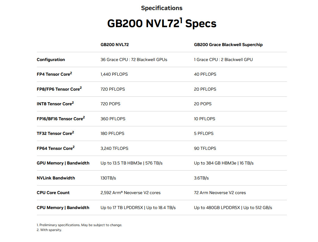
Nvidia started to show specs (
View: https://www.youtube.com/watch?v=f8DKD78BrQA), for the GB200:

GB200_NVL72_specs.jpg


Already out of the tera numbers for the under 64 bits operation and accelerating the new ultra low precision weight model started to use recently (only 16 different weights at 4 bits)

For comparison,
H200 sxm vs GB 200

Int 8 / float 8: 396 vs 20,000
FP16: 2000 vs 10,000
TF32: 989 vs 5000

An mi300x is in the 1300 (2600 for two of them ?) for FP16 and 2600 for FP8 for what they call peak performance

PFLOPS are quadrillion (10 exposed in 15), Nvidia is now talking in 40 quadrillion of operation in one second, in that spec sheet NVLink bandwith is now higher than the M2 ultra interconnect of 2.5TB/s....

Not having TSMC N3 sound a bit like a surprise to me....
 
Last edited:
Nvidia started to show specs (
View: https://www.youtube.com/watch?v=f8DKD78BrQA), for the GB200:

View attachment 642629

Already out of the tera numbers for the under 64 bits operation and accelerating the new ultra low precision weight model started to use recently (only 16 different weights at 4 bits)

For comparison,
H200 sxm vs GB 200

Int 8 / float 8: 396 vs 20,000
FP16: 2000 vs 10,000
TF32: 989 vs 5000

An mi300x is in the 1300 (2600 for two of them ?) for FP16 and 2600 for FP8 for what they call peak performance

PFLOPS are quadrillion (10 exposed in 15), Nvidia is now talking in 40 quadrillion of operation in one second, in that spec sheet NVLink bandwith is now higher than the M2 ultra interconnect of 2.5TB/s....

Not having TSMC N3 sound a bit like a surprise to me....

Important to not that the 40 petaflop number is FP4, which is yet another data type meant to "improve" machine learning performance. Top performance lists like the TOP500 use Linpack FP32, which is 8x slower than FP4. Still, 5 petaflops from a single "superchip" is impressive.
"could"

i could be leather jacket man himself posting on [H].
Here's some more leather jacket man for you:

NVIDIA launched their DGX SuperPOD with GB200 processors this week, which hits nearly 1.5 exaflops of FP32 with only eight NVL72 cabinets. Frontier at Oak Ridge, by comparison, is comprised of 74 cabinets. Frontier is listed as having sustained performance of 1.1 exaflops on the most recent TOP500 list. NVL72 is a huge game changer when it comes to power usage, cooling requirements, and space requirements in supercomputing.
 
Back
Top